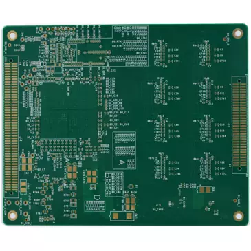
Product Name: 4 Layer PCB
Material: SY, KB
Layers: 4Layer
Thickness: 1.6mm
Copper thickness: 1/H/H/1oz
Surface technology: Glod
Solder mask: Green
Silk screen: White
Minimum line width/spacing: 4/4mil
Minimum through-hole: 0.2mm
Application: electronic product
What is 4 layer PCB?
4 layer PCB refers to a circuit printed board made of 4 layers of fiberglass.
4 layer PCB boards have a wide range of applications in multiple industries due to their complex structure and excellent performance. This type of circuit board can support higher circuit density and more complex designs, and whether in commercial, industrial, or research fields, 4 layer PCB is a key component for achieving innovative and high-performance solutions.
What is the difference between 4 layer PCB vs 2 layer PCB?
In the field of electronic manufacturing, choosing the appropriate type of PCB (printed circuit board) is crucial for meeting the needs of specific applications. 4 layer PCB and 2 layer PCB are two common types of PCB boards that differ significantly in terms of structure, performance, and cost. Understanding these differences can help PCB engineers and PCB designers make more appropriate choices.
The structural difference between 4 layer PCB and 2 layer PCB: 4 layer PCB consists of four conductive layers, while 2 layer PCB only has two. This means that 4 layer PCB can accommodate more traces and components, making it suitable for more complex circuit designs.
Electrical performance: Due to the fact that 4 layer PCB has more wiring layers, it can provide better signal integrity and lower crosstalk. This is particularly important for high-speed and high-frequency applications.
Thermal management: 4 layer PCBs typically have better thermal management capabilities. The additional inner layer can serve as a ground plane or power plane to help dissipate heat and improve the reliability of the components.
Size and weight: For the same circuit complexity, 4 layer PCB can achieve smaller size and lighter weight as it allows for higher wiring density.
Cost: Although 4 layer PCB provides more features and advantages, its cost is relatively high. This is mainly due to its more complex manufacturing process and material costs.
Design complexity: Designing 4 layer PCB requires a higher level of technical expertise and experience as it involves more interlayer connections and impedance control.
Testing and maintenance: Testing and maintenance of 4 layer PCB may be more difficult as fault diagnosis and repair typically require specialized equipment and technology.
Reliability: With appropriate design and manufacturing, 4 layer PCB can provide higher reliability, especially in harsh environments.
Environmental adaptability: 4 layer PCB is more suitable for applications with high environmental requirements, such as aerospace, military, and medical equipment.
Future Scalability: With the development of technology, 4 layer PCBs provide better scalability, making it easy to add new features and characteristics.
Both 4 layer PCB and 2 layer PCB have their own advantages and limitations. The choice of PCB type depends on specific application requirements, budget constraints, and performance requirements.

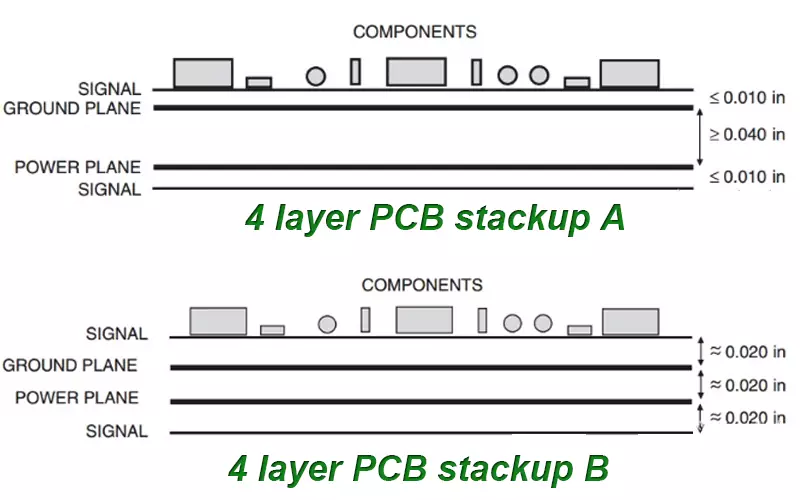
4 layer PCB stack refers to combining four layers of circuit boards through stacking technology. 4 layer PCB stack can reduce the volume and weight of the circuit board, and increase its circuit density. Meanwhile, due to the fact that the 4 layer PCB stack can also improve the signal integrity of the circuit board, it has been widely used in the field of high-speed transmission.
In the PCB stack 4 layer, since the layers need to be connected through conductive holes, it is necessary to set up solder pads and conductive holes inside and outside the circuit board respectively. In general, the internal layers of 4 layer PCB stack are designed with alternating signal and ground layers, while the external layers are typically designed with a combination of power and ground layers.
The thickness of 4 layer PCB stack is usually determined by the thickness of the internal layers and the diameter of the conductive holes. In general, the thickness of the internal layers of the PCB stack 4 layer is between 0.1mm and 0.2mm, and the diameter of the conductive holes is between 0.2mm and 0.3mm. The thickness of the outer layer is usually between 0.2mm and 0.3mm.
In PCB stack 4 layer, the thickness of the internal layers and the diameter of the conductive holes will have an impact on the performance of the circuit board. Therefore, when designing 4 layer PCB stack, it is necessary to choose according to actual needs and application scenarios.
4 layer PCB stack is a high-density, high-performance circuit board design method that can significantly improve the signal integrity and transmission speed of the circuit board. When 4 layer PCB stackup, it is important to pay attention to the thickness of the internal layers and the diameter of the conductive holes to ensure the performance and stability of the circuit board.
Product Name: 4 Layer PCB
Material: SY, KB
Layers: 4Layer
Thickness: 1.6mm
Copper thickness: 1/H/H/1oz
Surface technology: Glod
Solder mask: Green
Silk screen: White
Minimum line width/spacing: 4/4mil
Minimum through-hole: 0.2mm
Application: electronic product
iPCB Corporation provides support for PCB Prototype and Electronic Manufacturing. You can request consultation or quotation for PCB, PCBA and ODM here, please contact email: sales@ipcb.com
We will respond very quickly.