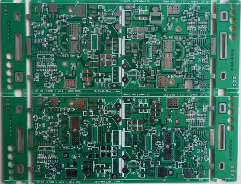
Copper pour is a crucial aspect of PCB design, utilized in various software, both domestic like Qingyuefeng and international options like Protel and PowerPCB. This technique involves filling the unused areas of a PCB with solid copper, known as copper flood. The benefits of copper pour include reducing ground impedance, enhancing noise immunity, lowering voltage drop, and improving power efficiency. Additionally, it connects to the ground, minimizing loop area, and most PCB manufacturers recommend filling open spaces with copper or mesh ground to prevent warping during soldering. However, if not managed properly, copper pour can lead to issues. So, is copper pour more beneficial than detrimental?

PCB
In high-frequency PCBs, the distributed capacitance of traces on a printed circuit board (PCB) can play a significant role. If the trace length exceeds 1/20 of the wavelength corresponding to the noise frequency, it can act like an antenna, emitting noise outward. Poor grounding in copper pour can exacerbate this issue, so it's crucial to ensure good grounding by using vias spaced less than λ/20 from the ground plane in multilayer boards. When executed correctly, copper pour not only increases current capacity but also serves as an interference shield.
There are generally two basic types of copper pour: large-area pour and grid copper. The choice between the two isn’t straightforward. Large-area copper can effectively increase current and provide shielding, but it can also cause warping during wave soldering, potentially leading to bubbling. Typically, several slots are created in large-area pours to alleviate bubbling. Grid copper primarily serves as a shield, with reduced capacity for current increase. From a thermal perspective, grid copper is advantageous as it lowers the heated surface area and provides some electromagnetic shielding. However, the mesh consists of traces oriented in different directions, and trace width relative to the circuit board's operational frequency is critical. If the operational frequency isn’t high, the grid's impact might be minimal. However, when the electrical length aligns with the operating frequency, it can severely disrupt circuit functionality, leading to unintended interference. Thus, I advise colleagues using grid copper to select based on their specific PCB design needs, rather than adhering rigidly to one method. High-frequency circuits that require superior noise immunity should lean toward grid copper, while low-frequency, high-current circuits can benefit from full copper pour.
To optimize copper pour for desired outcomes, here are some essential considerations:
Separate Grounding: If multiple ground types exist (SGND, AGND, GND), use the main ground as a reference for independent copper pours, ensuring digital and analog grounds are kept separate. Before pouring, also widen the corresponding power connections (e.g., 5.0V, 3.3V) to create various shapes.
Single-point Connections: Connect different grounds using zero-ohm resistors, ferrite beads, or inductors.
Surrounding Crystal Oscillators: Since oscillators act as high-frequency emitters, surround them with copper and ground their housings separately.
Islands (Dead Zones): If large islands exist, define a ground via to connect them; this is a minor task.
Ground Trace Priority: Treat ground traces with equal importance during routing; avoid relying on vias added post-copper pour to connect ground pins, as this leads to poor performance.
Avoid Sharp Corners: Try to eliminate sharp angles (≤180 degrees) to prevent them from functioning as radiation antennas. Instead, use rounded edges.
Avoid Pouring in Inner Layers: Do not pour copper in open areas of inner layers on multilayer boards, as achieving proper grounding is challenging.
Grounding Metal Components: Ensure that any internal metal parts, like heat sinks or reinforcing bars, have good grounding.
Ensure Grounding of Heat Sinks: The heat sink of three-terminal regulators must be well-grounded, and grounding isolation around oscillators is essential.
In summary, when grounding issues related to copper pour are managed properly, the advantages clearly outweigh the disadvantages. Effective copper pour can reduce the return area of signal lines and minimize electromagnetic interference.