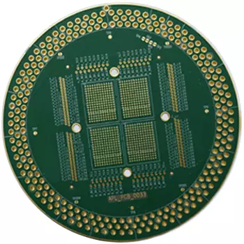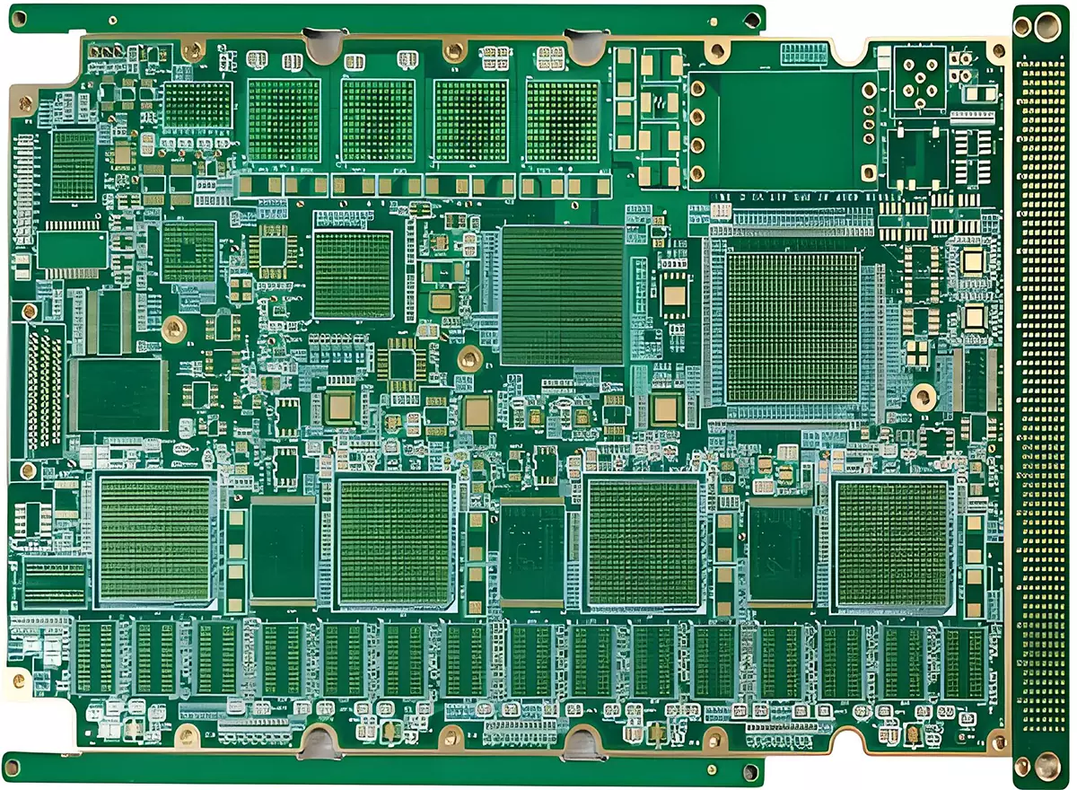
Product Name: Bare PCB
Material: FR-4
Quality standard: IPC 6012
Layers: 1L, 2L, Multilayer
Thickness: 1.6mm
Copper thickness: 1oz
Surface technology: gold, hasl
Solder mask: green, red, blue, black, white
Screen printing: black, white
Application: Electronic Products
There are many types of PCB circuit board, among which Bare PCB is the most common. So, what is Bare PCB? Simply put, it is a PCB board that has not undergone chemical etching, drilling, good surface treatment, and other steps. The biggest difference between it and a finished circuit board is that it has not been soldered or assembled.
Bare PCB is a PCB circuit board without components, because the components soldered onto Bare PCB are called PCBA. If there is no soldering, a single PCB board is called Bare PCB.
Bare PCB has no function, only after SMT and soldering the components onto Bare PCB can the circuit function.
Bare PCB raw materials: Copper clad laminates are substrate materials used to make printed circuit board. In addition to supporting various components, they can also achieve electrical connections or insulation between them. Bare PCB is almost present in every electronic device. If there are electronic components in a certain device, they are all embedded on PCB of different sizes. In addition to fixing various small parts, the main function of PCB is to provide electrical connections between the various components on top.
As one of the most important and fundamental components in electronic components, Bare PCB circuit board play an increasingly important role in modern electronic devices, and are widely used in fields such as telephones, computers, televisions, mobile devices, and automotive electronics.
What are the advantages of Bare PCB? Firstly, it enables electronic designers to test circuits and try new ideas at a very low cost. Once the circuit is correct, it can be transferred to the finished circuit board for soldering and assembly. Secondly, when the public PCB cannot meet the design requirements, Bare PCB can be used for self-made, which is also the reason why DIY electronics enthusiasts widely use Bare PCB.
There are also some drawbacks to using Bare PCB. Firstly, even excellent designers cannot guarantee the overall quality and stability of Bare PCB design, therefore detailed testing and inspection are required. Secondly, for small-scale production and personal use, using Bare PCB may be more cost-effective, but for mass production, the cost of producing Bare PCB will become relatively high.

Bare PCB circuit board
Composition and Function of Bare PCB
Bare PCB is mainly composed of insulating substrate, conductive layer, and solder pads. Insulating substrates are usually made of materials such as glass fiber and epoxy resin, which provide mechanical support and electrical insulation for circuit board. The conductive layer is a conductive pattern formed on an insulating substrate through chemical or physical methods, used to connect the pins of electronic components and achieve circuit connection. A solder pad is a specific area on a conductive layer used for soldering electronic components.
The main function of Bare PCB is to provide stable and reliable electrical connections and mechanical support for electronic components. By soldering the pins of electronic components onto the conductive layer of the PCB, electrical connections between electronic components can be achieved, thereby forming a complete circuit system. In addition, PCB also have good insulation and thermal conductivity, which can effectively protect circuit systems from external interference and overheating damage.
Types and Manufacturing Processes of Bare PCB
According to factors such as substrate type, conductive layer number, and application field, PCB can be divided into various types, such as single-layer PCB board, double-layer PCB board, multi-layer PCB board, etc. Different types of Bare PCB also have differences in manufacturing processes and performance. For example, multilayer board can achieve more complex circuit designs and higher circuit densities by stacking multiple conductive layers between insulating substrates.
In terms of manufacturing process, the production of Bare PCB usually includes multiple steps such as circuit design, graphic processing, substrate cutting, drilling, electroplating, etching, etc. Among them, circuit design is the first step in the manufacturing process, which determines the conductive pattern and component layout of the PCB circuit board. Subsequently, the circuit design is converted into actual production drawings through graphic processing, followed by mechanical processing such as substrate cutting and drilling. Finally, precise conductive patterns and pads are formed through chemical treatment steps such as electroplating and etching.
As a carrier of electronic components and a provider of circuit connections, Bare PCB plays a crucial role in electronic devices. It not only affects the performance and stability of electronic devices, but also directly relates to the reliability and service life of products. Therefore, it is crucial to choose appropriate PCB materials and manufacturing processes in the design and manufacturing process of electronic devices.
Bare PCB circuit board is an indispensable component in electronic devices. Understanding the basic concepts, composition, types, and manufacturing processes of Bare PCB is of great significance for procurement personnel from electronic equipment manufacturers. When choosing a Bare PCB supplier, factors such as technical strength, product quality, and production capacity should be comprehensively considered to ensure that the purchased Bare PCB can meet the actual needs of electronic devices.
Product Name: Bare PCB
Material: FR-4
Quality standard: IPC 6012
Layers: 1L, 2L, Multilayer
Thickness: 1.6mm
Copper thickness: 1oz
Surface technology: gold, hasl
Solder mask: green, red, blue, black, white
Screen printing: black, white
Application: Electronic Products
iPCB Corporation provides support for PCB Prototype and Electronic Manufacturing. You can request consultation or quotation for PCB, PCBA and ODM here, please contact email: sales@ipcb.com
We will respond very quickly.