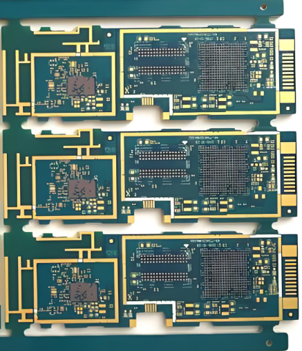
The performance and reliability of electronic devices heavily rely on the meticulous design and layout of the printed circuit board. By adhering to fundamental principles of PCB layout and routing, engineers can minimize noise, enhance signal integrity, and ultimately produce more efficient and dependable circuits. Here's an updated and refined overview of the key principles to follow when designing circuit layouts:

PCB Routing
1. Component Placement Strategies
The proximity of related components plays a critical role in minimizing interference. For example, components such as clock generators, crystal oscillators, and the CPU clock input should be placed as close together as possible to reduce noise susceptibility. Conversely, it's crucial to isolate high-current switching circuits from sensitive areas like the control and memory circuits of microcontrollers (e.g., ROM, RAM). In instances where these circuits can be segmented onto separate PCBs, it is advisable to do so as this further mitigates interference and bolsters circuit reliability.
2. Strategic Decoupling Capacitor Installation
Correctly positioning decoupling capacitors is essential to stabilize voltage levels and combat noise. Large inductance in PCB traces may cause significant switching noise spikes on the Vcc trace placing a 0.1 µF decoupling capacitor directly between VCC and ground can effectively counteract this issue. For surface mount configurations, opt for chip capacitors situated close to the components, ideally leveraging ceramic capacitors due to their low equivalent series inductance (ESL) and superior performance in high-frequency applications.
Recommendations for Decoupling Capacitors:
A 100 µF electrolytic capacitor should ideally be connected across the power input. Larger capacitance is beneficial if space allows.
Place a 0.01 µF ceramic capacitor next to each integrated circuit. If space is limited, consider using tantalum capacitors (1-10 µF) for every ten chips as a compromise.
Always connect decoupling capacitors for components sensitive to noise, ensuring leads are kept as short as possible especially for high-frequency bypass capacitors.
3. Grounding Practices for Enhanced Stability
A well-structured grounding scheme is critical to the overall performance of PCB designs. There are several types of grounding that should be conceptualized: system ground, shield ground, logic ground, and analog ground. When laying out grounds:
Separate Logic and Analog Grounds: To reduce interference, keep analog and digital grounds distinct and connect them to appropriate power ground ties. Utilize thicker traces for analog grounds to minimize impedance and ensure that grounding areas are maximized.
Use of Opto-couplers: To isolate input and output signals effectively from the microcontroller, consider implementing opto-couplers.
Implement Ground Loops Wisely: The ground trace should ideally form a closed loop to enhance noise immunity. However, for frequencies below 1 MHz, single-point grounding can mitigate circulating currents, while multi-point grounding may be more effective for higher frequencies (above 10 MHz) to reduce impedance.
4. Trace Width and Routing Considerations
The width of the power and ground traces is vital for managing current flow. Ensure that the width of main ground traces is at least 2-3 mm and for component pins about 1.5 mm. Power traces should mirror the direction of data lines to maintain consistency and performance.
Data Line Guidelines: Data lines should be at least 0.3 mm (12 mil) wide, with 0.46–0.5 mm (18-20 mil) being preferable to minimize impedance and enhance signal integrity.
Minimizing Via Count: Be mindful that each via introduces approximately 10 pF of capacitance, which can significantly affect high-frequency performance. Reducing the number of vias not only limits this interference but also enhances the mechanical integrity of the PCB.
Conclusion
Designing an effective PCB layout is a blend of adhering to sound engineering principles and staying attuned to the latest industry practices. By focusing on strategic component placement, proper decoupling techniques, thoughtful grounding practices, and careful routing, engineers can significantly enhance the robustness and reliability of their circuit boards. With newer materials and technologies continually emerging in the PCB industry, staying updated on best practices is essential for successful design and implementation in today's fast-evolving electronics landscape.