Share cost-effective products and high-quality services with customers. Contact Us


In the world of modern electronics, Ball Grid Array components and HDI PCBs go hand in hand. BGA packages, especially those with high pin counts, demand advanced routing techniques to ensure efficient connectivity and signal integrity. At IPCB, we specialize in designing HDI PCBs that accommodate complex BGA components, even when they handle high-speed or high-frequency signals. One of the critical challenges in such designs is implementing effective escape routing strategies while maintaining controlled impedance requirements.This article explores the key considerations and strategies for BGA escape routing in HDI PCBs, focusing on fine-pitch components and high-speed signal integrity.

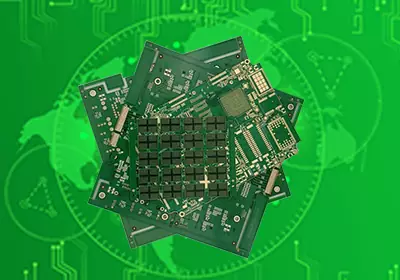
BGA Routing
Escape Routing Strategies for BGA Components
The escape routing strategy for BGA components largely depends on the pitch of the BGA, which determines the maximum trace width that can fit between solder pads. The minimum trace width, on the other hand, is influenced by manufacturing capabilities, layer stack-up, and impedance requirements.
For moderate-layer-count HDI PCBs, IPCB designers often employ a neck-down routing strategy for fine-pitch BGAs. Here's how it works:
First Row of Pads: Traces are routed directly from the exterior pads.
Second Row of Pads: Trace widths are slightly reduced to allow routing between the first row of pads.
Inner Rows: Traces are routed to interior layers using vias or micro-vias.
In most cases, two rows of pads can be routed per signal layer while maintaining controlled impedance and minimizing crosstalk.
Dog Bone Fanout Strategy
For BGAs with a pitch of 1 mm or less, the dog bone fanout strategy is a popular choice. This approach involves placing a secondary pad close to the BGA pad, connected by a short trace. A via is then placed on the secondary pad to route the trace to another layer.
Key advantages of the dog bone fanout strategy:
The connecting trace is covered by solder mask, eliminating the need for via plating or filling.
It is suitable for BGAs with pitches down to 0.8 mm.
However, for BGAs with pitches below 0.8 mm, this strategy becomes less effective due to smaller pad sizes and tighter spacing.
Micro-Via Strategy for Ultra-Fine-Pitch BGAs
For BGAs with pitches below 0.8 mm, traditional vias are often too large to fit within the limited space. This is where micro-vias come into play. Micro-vias, typically laser-drilled, offer several advantages over mechanically drilled vias:
Aspect Ratio: Micro-vias have an aspect ratio (via length divided by diameter) of less than 2, ensuring reliability and manufacturability. For example, on a 32-layer board with a 2-mil layer thickness, the micro-via diameter cannot be less than 1 mil.
Via Depth: Unlike traditional vias that span multiple layers, micro-vias typically span only one or two layers. This reduces routing congestion and improves signal integrity.
Laser Drilling: Laser drilling is more precise and cost-effective for creating small-diameter vias compared to mechanical drilling, which is limited to sizes above 8 mils.
For ultra-fine-pitch BGAs (e.g., 0.5 mm pitch), IPCB designers use micro-vias-in-pads to route traces to inner layers while maintaining adequate clearance between pads.
Stacked and Staggered Micro-Vias
In high-layer-count HDI PCBs, designers often use stacked or staggered micro-vias to achieve the necessary routing density:
Stacked Micro-Vias: These are vertically aligned micro-vias that span multiple layers, offering a compact routing solution.
Staggered Micro-Vias: These are offset micro-vias that reduce stress concentration and improve reliability.
IPCB adheres to the IPC 6012 standard to ensure the reliability of micro-vias in high-density designs.
Controlled Impedance in BGA Routing
When BGAs handle high-speed signals, maintaining controlled impedance is critical. The impedance of the fanout section, which connects the BGA pad to a longer trace, is influenced by the trace length and the parasitic inductance and capacitance of the micro-via.
IPCB recommends the following guidelines for impedance control:
For traces shorter than the wavelength of the highest-frequency signal, the fanout portion can often be ignored. For example, for a 20 GHz signal on an FR-4 substrate, a 0.73 mm stripline is considered critical.
In high-layer-count designs, trace widths may need to be reduced to maintain the target impedance.
Conclusion
Designing HDI PCBs with BGA components requires a deep understanding of escape routing strategies, micro-via technology, and impedance control. At IPCB, we leverage cutting-edge design techniques and advanced manufacturing capabilities to create high-performance PCBs for a wide range of applications, from consumer electronics to aerospace systems.
Whether you're working with fine-pitch BGAs or high-speed signals, IPCB ensures your design is fully manufacturable and optimized for performance. Contact us today to learn more about our expertise in HDI PCB design and manufacturing.