Share cost-effective products and high-quality services with customers. Contact Us


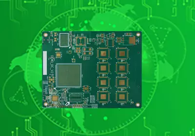
When a multilayer PCB becomes crowded around fine-pitch components, the problem is often not a lack of layers but a lack of usable routing space. A conventional through-hole via passes through the entire board, occupying space on every layer it crosses even when the electrical connection only needs to reach one internal layer. A blind via PCB provides another option by connecting an outer layer to a specific internal layer without extending through the complete board.
This becomes particularly useful around BGA packages and other high-density areas. A blind via can make a short vertical transition and leave deeper layers available for other signals. In HDI construction, this approach is combined with thin dielectric layers and small via structures to create additional routing channels within a limited board area.
The value of a blind via is therefore mainly about how it interacts with the entire layer stack. The hole itself is only one part of the design. The starting layer, target layer, drilling process, pad geometry, dielectric thickness and routing around the via all determine whether the structure actually provides an advantage.
Why Blind Vias Are Used
Consider a fine-pitch BGA where several rows of pads need to escape to different PCB layers. If every connection uses a through-hole via, the via barrels and associated clearances can consume routing channels across the complete stack. Some of those connections may only need to reach the first or second internal layer.
A blind via allows that transition to stop where the connection is needed. The unused layers below the target layer are no longer occupied by that particular via, creating additional space for traces and other connections. This is one reason blind vias are frequently used for dense BGA fanout and other high-density routing situations.
The benefit becomes more apparent as component pitch decreases. When the space between pads is limited, even a small change in via diameter, pad size or clearance can determine how many traces can escape from the component area. Blind vias and microvias can provide shorter layer transitions that make these breakout patterns possible.
They can also be useful outside BGA fanout. A designer may need a controlled connection between an outer signal layer and a particular internal reference or routing layer, while keeping other layers free. In some high-speed or RF constructions, mechanically drilled blind vias can also be used when the required electrical or mechanical structure calls for a defined termination rather than a full through-hole connection.
This does not mean that blind vias should automatically replace through-hole vias. A through-hole structure is usually simpler to manufacture, and adding blind or buried structures can introduce additional fabrication steps. The practical question is whether the routing, mechanical or electrical requirement justifies the additional complexity.
How a Blind Via Fits Into the PCB Stackup
The most important decision is where the blind via begins and where it ends. For example, a connection from the top copper layer to the first inner layer is a relatively simple blind structure. A connection that skips one or more layers requires a different construction and must be checked against the fabrication process.
This makes stack-up planning an important part of blind via design. The designer cannot determine the via only from the schematic or PCB layout. The dielectric thickness between the relevant layers, copper thickness, target pad and available drilling process all affect the finished structure.
There are several ways to manufacture blind vias. Some mechanically drilled blind structures are produced through sub-lamination and additional drilling and plating operations. Laser-drilled microvias are commonly created in thin buildup dielectric during sequential lamination. The two approaches have different process limits and should not be treated as interchangeable.
This is also where the distinction between blind via and microvia matters. A blind via is defined by its relationship to the board surfaces and internal layers. A microvia is a much smaller via structure with a specific definition in HDI standards. IPC material describes a microvia as a blind hole with a diameter of up to 150 μm, so a blind via is not automatically a microvia simply because it does not pass through the board.
In an HDI board, the two concepts frequently overlap. A laser-drilled microvia on an outer buildup layer can be a blind via, while a larger mechanically drilled blind via can also exist in a multilayer PCB. The design documentation should therefore specify the actual layer span and manufacturing structure rather than relying on terminology alone.

Design Around the Via Instead of the Hole
A blind via should be evaluated together with its surrounding copper. The pad needs enough area to provide a reliable connection to the target layer, while clearance from neighboring copper must remain within the fabrication rules. Registration between the drilled feature and the target land is also important, particularly when the via diameter becomes small.
The routing pattern around a blind via often determines whether the structure is worthwhile. In a dense BGA fanout, changing the position of a blind via can open a routing channel that would otherwise be blocked. HDI design techniques can use staggered, stacked or skip-via arrangements to create different paths through the layer structure. The appropriate arrangement depends on the package geometry and the chosen stack-up.
For high-speed signals, the via transition also becomes part of the electrical path. A change between routing layers can alter the local impedance and affect the return-current path. The surrounding reference plane, via placement and signal geometry should therefore be reviewed together rather than treating the blind via purely as a mechanical connection.
Via-in-pad is another situation where blind or microvia structures can become useful. A connection can be made directly from a component pad to an internal layer, which can shorten the breakout path and save surface routing space. When the via needs to be filled and planarized for assembly, however, the fabrication process becomes more involved. IPC documentation identifies via plugging and planarization as important processes for HDI, microvia and via-in-pad structures.
The design should also avoid using blind vias simply to compensate for an inefficient stack-up. Sometimes a different layer assignment, component placement or routing strategy can solve the problem without introducing another fabrication step. Blind vias are most useful when the layer-to-layer connection they provide has a clear purpose.
Manufacturing and Reliability
Once blind vias are included in the design, the PCB manufacturing process needs to be considered before the layout is released. A fabricator needs to know the required via span, drilling method, hole size, target land dimensions and stack-up. Mechanically drilled blind and buried vias can require additional lamination and drilling operations, while HDI microvias are commonly produced through sequential buildup.
Laser drilling is widely used for HDI microvias because it can create controlled-depth holes in thin dielectric layers. After the hole is formed, metallization establishes the electrical connection. For stacked structures, the quality of each successive interconnection matters because several microvia interfaces may form one vertical electrical path.
Copper plating is therefore a major reliability consideration. The finished structure needs adequate conductive coverage and must tolerate the thermal and mechanical conditions expected during PCB assembly and operation. Registration is equally important because a small alignment error can reduce the available connection area between the via and target land.
Via filling may be required when the structure is used beneath component pads or when another buildup layer must be formed over the via. A filled and planarized via can provide a suitable surface for subsequent processing, but it adds another manufacturing requirement that needs to be included in the fabrication specification.
For this reason, the best blind via PCB design is not necessarily the one with the smallest holes or the largest number of HDI structures. A practical design balances routing density against stack-up complexity, manufacturing capability, assembly requirements and long-term reliability. When the blind via structure is chosen together with the PCB stack-up and routing strategy, it can solve dense interconnection problems without adding unnecessary complexity to the board.