Share cost-effective products and high-quality services with customers. Contact Us


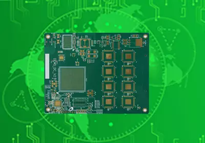
A ceramic multilayer PCB is a multilayer circuit substrate that uses ceramic materials as the insulating structure and integrates conductive patterns across multiple layers. Unlike a conventional multilayer PCB built by laminating copper-clad materials and dielectric prepregs, a multilayer ceramic circuit is typically created from unfired ceramic sheets, conductive materials, and vertical interconnections that are processed together and then fired into a solid ceramic structure.
This difference is important because the ceramic material is not simply replacing the dielectric material used in a conventional PCB. In a ceramic multilayer structure, the insulating layers, internal conductors, vias, cavities, and other features can be formed as part of a co-fired structure. This allows electrical connections to be routed not only across the top and bottom surfaces but also through internal ceramic layers.
Two technologies are particularly important when discussing multilayer ceramic circuits: LTCC, or Low Temperature Co-Fired Ceramic, and HTCC, or High Temperature Co-Fired Ceramic. Both use ceramic green sheets that are structured, stacked, laminated, and fired, but their material systems, firing temperatures, conductor systems, and typical application requirements are different. Fraunhofer IKTS describes LTCC and HTCC as ceramic multilayer technologies based on green-sheet processing, via formation, conductor printing, stacking, lamination, and sintering.
Why Use a Multilayer Ceramic Structure?
The main reason to use a ceramic multilayer PCB is that some electronic systems need electrical, thermal, mechanical, or environmental characteristics that are difficult to obtain from a conventional organic PCB structure.
Ceramic materials can provide high thermal stability, good dimensional stability, and useful electrical characteristics for demanding applications. When these properties are combined with a multilayer structure, the circuit can be integrated into a compact ceramic substrate instead of relying entirely on surface-level routing.
The multilayer structure also changes how the circuit can be arranged. A designer can dedicate internal layers to power, ground, signal routing, or other functional structures and connect them through vertical vias. This makes it possible to place electrical connections within the ceramic body rather than routing every connection across the outer surface.
The benefit becomes particularly relevant in compact RF and microwave assemblies. An RF module may require controlled signal paths, ground structures, short interconnections, and a compact physical footprint. A multilayer ceramic substrate can combine these functions within a relatively small three-dimensional structure. Egide notes that the multilayer structure of HTCC can be used similarly to a PCB, with ceramic layers serving as routing, power, ground, and signal layers connected through vias.
Thermal behavior is another consideration. The actual thermal performance depends strongly on the selected ceramic material and construction, so ceramic should not be treated as a single material category with one fixed thermal conductivity. Alumina, aluminum nitride, silicon nitride, and other ceramic systems have different properties and are selected according to the electrical, thermal, mechanical, and manufacturing requirements of the application.
The choice of ceramic technology therefore depends on the complete system rather than simply on the number of PCB layers. A high-frequency module, high-temperature package, sensor substrate, power-related structure, and hermetic electronic package may all use ceramic multilayer technology for different reasons.

LTCC and HTCC in Multilayer Ceramic PCB Manufacturing
LTCC and HTCC are both based on co-fired ceramic technology, but they are not interchangeable processes.
LTCC uses ceramic and glass-ceramic material systems that can be fired at lower temperatures than traditional high-temperature ceramic systems. The lower firing temperature makes it possible to use conductive materials that would not be suitable for much higher firing temperatures. LTCC is therefore widely associated with compact multilayer structures, high-frequency modules, and applications where integrated passive components and dense internal routing are valuable. Egide describes LTCC as generally suitable for RF, microwave, and millimeter-wave applications because of the electrical characteristics of its glass-ceramic material system.
HTCC uses a higher-temperature firing process and commonly relies on refractory metal conductors that can withstand the required sintering conditions. This manufacturing route produces a robust ceramic structure and is widely used where mechanical strength, thermal stability, hermeticity, and harsh-environment performance are important. NIKKO's HTCC multilayer substrate information, for example, describes alumina-based multilayer circuit substrates and provides examples of high-temperature and low-loss ceramic characteristics.
The distinction between LTCC and HTCC is therefore more meaningful than simply comparing their firing temperatures. The ceramic composition, conductor material, internal circuit design, required mechanical characteristics, RF requirements, thermal environment, and packaging requirements all influence which process is appropriate.
A typical ceramic multilayer manufacturing sequence starts with ceramic powder that is processed into thin green sheets. The sheets are then cut or patterned according to the required circuit structure. Vias can be formed through the green sheets and filled with conductive material to provide vertical electrical connections. Conductive patterns are printed onto individual layers, after which the layers are aligned and stacked.
The stacked structure is laminated before being placed into a firing process. During sintering, the ceramic and conductive structures form a consolidated multilayer body. Fraunhofer IKTS describes this process as converting the processed green sheets into a monolithic ceramic body through lamination and sintering. KYOCERA similarly describes powder preparation, tape casting, punching, via filling, screen printing, lamination, co-firing, plating, singulation, and inspection as part of its ceramic multilayer package manufacturing process.
This process also explains why ceramic multilayer PCB manufacturing cannot simply copy the workflow used for a conventional FR-4 multilayer board. The circuit pattern is created before firing, and the entire stack undergoes a significant thermal process. Dimensional changes, material compatibility, conductor behavior, layer alignment, via formation, and sintering conditions therefore need to be considered during design.
Design and Manufacturing Considerations
Designing a ceramic multilayer PCB requires closer coordination between electrical requirements and manufacturing conditions. The designer needs to know the ceramic material system, layer thickness, conductor structure, via technology, minimum feature sizes, and expected dimensional tolerances before finalizing the layout.
Internal vias are especially important because they provide the vertical connections that make multilayer ceramic routing possible. Their diameter, pitch, pad dimensions, relationship with adjacent conductors, and distance from the substrate edge all depend on the manufacturing process. NIKKO's published HTCC design guidelines, for example, provide specific design ranges for layer count, via diameter, via pitch, line width, line spacing, and edge clearances. These values are examples of one manufacturer's process rather than universal specifications for every ceramic multilayer PCB.
The same principle applies to line width and spacing. Ceramic multilayer technology can support relatively fine internal structures, but the achievable geometry depends on the material system and fabrication process. A design that is technically possible on one production line may require different dimensions on another. The manufacturing capability should therefore be established before committing to very small traces, narrow spacing, or dense via structures.
Dimensional control is also important because the ceramic body is formed through firing. The relationship between the unfired green-sheet dimensions and the final sintered dimensions needs to be accounted for in the manufacturing process. This is one reason ceramic multilayer fabrication requires process-specific design rules rather than relying only on general PCB design rules.
Electrical performance needs similar attention. For RF and microwave applications, internal signal paths, ground structures, dielectric properties, conductor geometry, and layer spacing all influence the behavior of the finished circuit. A ceramic multilayer substrate can provide a compact environment for high-frequency routing, but the RF design still needs controlled impedance, appropriate grounding, and carefully managed transitions.
Thermal and mechanical requirements should also be considered together. Ceramic substrates may be selected because they can operate in demanding environments, but the specific ceramic material, metallization, package structure, and assembly process determine the final performance. The ceramic substrate should therefore be treated as part of the complete electronic assembly rather than as an isolated PCB material.
Applications and Final Considerations
Ceramic multilayer PCBs are used when the combination of multilayer routing and ceramic material properties provides a practical solution for the electronic system. Applications can include RF and microwave modules, sensor packages, compact electronic packages, high-temperature electronics, and other assemblies where conventional organic PCB structures may not provide the required combination of electrical, thermal, mechanical, or environmental performance.
RF applications are particularly relevant because ceramic multilayer structures can place signal, ground, and other functional layers within a compact substrate. High-frequency modules may also benefit from short internal connections and controlled physical structures. LTCC is commonly associated with RF and microwave applications, while HTCC is frequently used where higher-temperature processing and robust ceramic structures are required.
The manufacturing method ultimately determines much of what can be achieved. LTCC and HTCC are not simply alternative names for ceramic PCBs; they represent different material and processing systems with different conductor requirements and application characteristics. Other ceramic PCB processes, including DBC, DPC, and AMB, are also used for ceramic substrates, but they are generally associated with different structures and application requirements rather than being direct substitutes for multilayer co-fired ceramic technology. Current industry references distinguish these processes from LTCC and HTCC when discussing multilayer ceramic circuits.
For this reason, selecting a ceramic multilayer PCB begins with the requirements of the complete electronic system. Operating temperature, frequency, thermal load, electrical isolation, routing density, package dimensions, mechanical strength, and manufacturing volume all influence the appropriate ceramic material and fabrication technology.