Share cost-effective products and high-quality services with customers. Contact Us


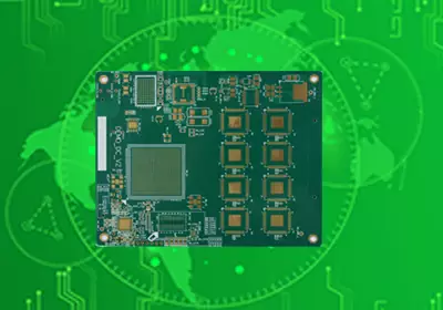
A circuit board via is a copper-plated hole used to establish electrical connections between conductive layers within a printed circuit board (PCB). Vias are an essential part of multilayer PCB design because they allow signals, power, and ground connections to transition vertically between different copper layers, eliminating the need to route every connection on a single layer.
A circuit board via is essentially a conductive interconnection structure between copper layers. During PCB manufacturing, a hole is first drilled or formed in the board material, after which copper is plated onto the hole wall. The resulting conductive copper barrel connects the copper features assigned to the via on different layers.
A standard via consists of a mechanically drilled or laser-drilled hole, a copper-plated barrel, and copper pads surrounding the connection points. On layers where the via does not need to make electrical contact with the surrounding copper plane, an isolation clearance known as an antipad is provided.
This structure allows a signal trace to transition from one layer to another. The same principle applies to power and ground connections. Via arrays can also provide thermal paths that transfer heat generated by components to underlying copper planes.
Without vias, multilayer PCB routing would be severely restricted. Traces would have to remain on a single conductive layer, or extensive external wiring would be required. The simplest via extends through the entire PCB, while more advanced via structures connect only selected layers. Through vias, blind vias, buried vias, and microvias address different routing and packaging requirements.
Via selection should take into account the PCB thickness, layer count, routing density, component lead pitch, signal integrity requirements, thermal conditions, and the manufacturing capabilities of the PCB fabricator.
Through Vias
Through vias are the most conventional type of circuit board via. They extend from one external surface of the PCB through the entire board thickness and can establish connections with selected copper layers along their path.
Through vias can be manufactured using mature mechanical drilling and copper plating processes, making them widely used in conventional multilayer PCBs. Typical applications include power connections, ground reinforcement, signal layer transitions, and general-purpose routing.
Their primary limitation is that they occupy space on layers where no electrical connection is required. Because a through via extends through the entire stackup, sufficient clearance must be provided around the via on the intermediate layers. In high-density multilayer layouts, this can significantly reduce the available routing area.
In high-speed PCB designs, through vias can also introduce unwanted electrical discontinuities. The portion of the via extending beyond the signal transition point forms a via stub. At high frequencies, a long via stub can behave as a resonant structure and cause signal reflections, resulting in signal integrity problems.
Blind Vias
Blind vias connect an outer layer to one or more inner layers without extending through the entire PCB. The via is visible from its starting surface, while its termination point is located within the PCB stackup.
The primary advantage of blind vias is that they do not consume routing space through the entire board thickness. They are particularly useful when routing density is high and conventional through vias create excessive congestion.
Blind vias are widely used in HDI (High-Density Interconnect) PCBs and other high-density designs. They provide greater flexibility for BGA fanout routing and allow designers to use the inner routing layers more efficiently.
Depending on their dimensions and structure, blind vias can be manufactured using different processes. Some structures can be produced using controlled-depth mechanical drilling, while microvia structures are typically formed using laser drilling.
Because a blind via does not extend through the entire board, its drilling depth must be precisely controlled. Registration between the via and the target pad is also critical, particularly as via dimensions become increasingly smaller.
Buried Vias
Buried vias connect two or more internal copper layers without reaching either external surface of the PCB. After the PCB stackup has been laminated, the buried via is completely enclosed within the finished board.
Buried vias can free valuable space on the outer layers, allowing the internal routing structure to be optimized independently of component placement. They are particularly useful in highly complex multilayer PCBs where conventional through vias cannot provide sufficient routing capacity.
However, buried vias require a more complex manufacturing process. In many cases, the internal interconnections are fabricated within substructures first, after which these substructures are laminated together to form the complete PCB stackup. The additional processing steps and registration requirements increase manufacturing complexity and cost.
Therefore, buried vias should not be selected simply because they are technically feasible. The stackup and routing architecture should first be evaluated to determine whether the additional manufacturing complexity provides a meaningful design benefit.
Microvias and HDI PCB Design
Microvias are small-diameter via structures primarily used in High-Density Interconnect (HDI) PCB technology. According to the HDI design definition in IPC-2226A cited by Siemens, a microvia has a hole diameter of less than 0.15 mm, a pad diameter of less than 0.35 mm, a maximum aspect ratio of less than 1:1, and a relatively short interconnection depth.
Unlike conventional mechanically drilled vias, microvias are typically manufactured using laser drilling. Their small dimensions allow them to be placed in areas where conventional vias would consume excessive routing space.
Microvias are particularly suitable for fine-pitch BGA fanout routing and compact HDI designs. They can establish interconnections between an outer layer and the adjacent inner layer. When a connection must transition across multiple layers, stacked microvias or staggered microvias can be used.
Stacked microvias can achieve extremely high routing density, but they impose more demanding requirements on copper filling, layer-to-layer registration, and long-term reliability. Where the stackup and available routing space permit, staggered microvias can be used as an alternative structure.
For this reason, the microvia structure should be selected as part of the overall HDI stackup design rather than introduced as a last-minute solution during PCB layout.
Via-in-Pad PCB Design
Via-in-pad refers to placing a via directly within a component pad rather than positioning the via adjacent to the pad.
This structure is particularly beneficial for fine-pitch BGA packages because it reduces the space required for fanout routing. It can also shorten the electrical interconnection path and, for thermally demanding devices, provide a direct thermal path from the component to the copper structure underneath.
However, placing an open via directly in a solder pad can cause molten solder to flow into the via during reflow soldering, potentially resulting in solder joint defects and assembly problems. Therefore, when a flat, solderable surface is required, via-in-pad structures typically require via filling, copper capping, and planarization.
The selection of via filling materials and manufacturing processes should be based on the pad geometry, component package, thermal requirements, reliability requirements, and the PCB fabricator's process capabilities.
Thermal Vias for PCB Thermal Management
Not all vias are used for signal transmission. Thermal vias are specifically designed to transfer heat from components to underlying copper planes or other thermal management structures.
Thermal vias are typically placed underneath or around heat-generating components such as voltage regulators, MOSFETs, LEDs, and other power semiconductor devices. An array of thermal vias can establish a thermal conduction path between the component area and the internal or bottom copper plane.
The thermal performance of a via array does not simply improve by increasing the number of vias. Via diameter, via pitch, copper connections, PCB thickness, thermal interfaces, copper plane area, and the final heatsink or thermal dissipation structure all affect the overall heat-transfer path.
Therefore, thermal vias should be considered as part of the overall PCB thermal design rather than as isolated layout elements.
Via Design and Signal Integrity
A via introduces a vertical layer transition into an otherwise planar transmission line. At low frequencies, this generally has little effect on circuit performance. However, at high data rates or microwave frequencies, the via itself becomes part of the transmission structure. Its parasitic capacitance, parasitic inductance, and structural discontinuities can significantly affect signal quality.
Via stub length is a critical consideration. When a through via extends beyond the layer where the signal transitions, the unused portion forms a via stub. At high frequencies, this stub can behave as a resonant structure and cause signal reflections.
Designers can mitigate these effects by minimizing via stub length, selecting an appropriate via structure, optimizing the reference plane configuration, or using backdrilling when stringent signal integrity requirements apply.
The geometry of the via pad and antipad also affects the local impedance environment. In high-speed designs requiring controlled impedance, via dimensions should be designed in conjunction with trace width, dielectric thickness, reference-plane spacing, and the overall PCB stackup.
Via Spacing and Clearance
Via placement should not be evaluated based solely on the finished hole diameter. The complete via geometry includes the drilled hole, copper pad, annular ring, and the required clearance between the via structure and surrounding copper features.
The required dimensions depend on the PCB manufacturing process, stackup, copper thickness, registration capability, electrical requirements, and applicable design standards.
Smaller vias can provide greater routing flexibility, but reducing via dimensions generally increases manufacturing difficulty and places more demanding requirements on drilling, plating, registration, and inspection. Therefore, designers should not simply select the smallest possible via to maximize routing density.
A more practical approach is to use standard via dimensions that are compatible with the PCB fabricator's established process capabilities. Advanced via structures should be adopted only where they provide a clear electrical, mechanical, or routing benefit.

How to Select the Right circuit board via Type
The most practical approach is to use through vias whenever possible and upgrade to more complex via structures only when the design requires them.
When sufficient routing space is available and the design does not have stringent high-speed requirements, conventional through vias are generally adequate. When routing density becomes high and through vias become inefficient, blind vias can be considered. When additional routing flexibility is required within the inner layers without consuming valuable outer-layer space, buried vias may be evaluated.
When component pitch and routing density exceed the practical limits of conventional vias, microvias can provide significant advantages. They are particularly valuable in HDI PCBs and designs using compact, fine-pitch packages.
Via-in-pad can be considered when conventional fanout routing is difficult to implement or when the electrical and thermal benefits are sufficient to justify the additional manufacturing cost.
The final via selection should always be confirmed with the PCB fabricator because drilling specifications, aspect-ratio limitations, copper plating capabilities, registration tolerances, laser drilling capabilities, via filling processes, and minimum spacing requirements vary between manufacturing processes and suppliers.
Circuit board via Manufacturing
Via fabrication processes vary depending on the type of via being produced.
Through vias are generally manufactured using mechanical drilling, followed by copper plating of the hole walls. Blind and buried vias require more tightly controlled manufacturing sequences because drilling depth and layer-to-layer registration must be precisely controlled.
Microvias are typically produced using laser drilling, which requires precise control of laser parameters, target pad geometry, copper foil structure, and copper plating processes. In HDI PCB manufacturing, sequential lamination may be required to build additional dielectric layers and interconnection structures.
After drilling, the conductive structure must provide reliable electrical continuity. Hole-wall quality, copper thickness, registration accuracy, and plating integrity are all critical manufacturing factors. Via defects can result in intermittent electrical connections, opens, shorts, and long-term reliability issues.
Via Reliability
Via reliability depends on the mechanical and thermal stresses that the PCB experiences throughout its service life.
Temperature cycling causes different materials within the PCB to expand and contract at different rates.Because copper and the surrounding dielectric materials have different coefficients of thermal expansion (CTE), the copper-plated barrel or microvia structure can experience significant mechanical stress.
This issue is particularly important for high-aspect-ratio through vias and stacked microvias. Manufacturing quality, plating integrity, drilling quality, material selection, and temperature-cycling conditions all affect long-term via reliability.
For demanding applications, via structures should therefore be incorporated into the overall PCB reliability design rather than selected solely for routing convenience.
Although circuit board vias are physically small, they have a significant impact on PCB routing, signal integrity, thermal management, manufacturing cost, and long-term reliability.The optimal via design strategy is not to select the smallest or most technologically advanced via structure in every case.Instead, designers should select the simplest via technology that satisfies the electrical, thermal, mechanical, routing-density, and reliability requirements of the PCB while remaining compatible with the manufacturing process.