Share cost-effective products and high-quality services with customers. Contact Us


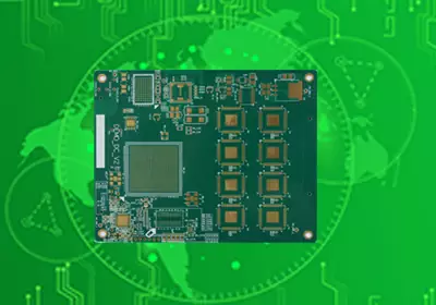
A circular pcb board is designed to fit products that require a round electronic assembly, such as LED modules, sensor units, compact control devices, and circular instrument panels. Unlike a rectangular PCB, its curved perimeter and limited usable area affect component placement, routing, mounting, and assembly. A successful design must therefore account for the product's mechanical geometry and electrical requirements from the beginning, rather than simply changing the outline of an existing board.
Mechanical Dimensions Define the Usable Circular PCB Board Area
The outside diameter is only one part of a circular PCB's mechanical design. The board may also require a central opening, mounting holes, edge notches, connector cutouts, or slots for alignment. Each feature reduces the available routing area and can influence the position of nearby components.
When designing a circular pcb board for a round enclosure, engineers should confirm the internal diameter, board thickness, mounting positions, and clearance around the finished assembly. The nominal board diameter alone does not guarantee a proper fit. Screw heads, retaining clips, connectors, and adjacent components may extend beyond the board surface and interfere with the housing.
Mechanical drawings should define the finished outline and critical tolerances clearly. For assemblies involving a central shaft, optical lens, speaker, or rotating component, the position of the opening is just as important as its diameter. Checking the circular pcb board against a three-dimensional enclosure model can reveal interference before fabrication begins.
Defining these dimensions early also reduces redesign risk. Moving a hole or changing the board perimeter after routing may require adjustments to copper traces, component footprints, and mounting hardware.
Component Placement and Routing Must Work With the Curve
The curved edge creates placement constraints that do not occur in the same way on a rectangular board. Rectangular components may leave unused pockets near the perimeter, while connectors and mounting hardware need sufficient clearance from the edge. Copper features must also remain within the fabrication limits for edge clearance and routed profiles.
A circular pcb board can benefit from radial placement when the product itself has a circular function. For example, LEDs may be arranged around a central point, or sensors may be distributed at defined angular intervals. However, a symmetrical component arrangement is not always the most efficient electrical layout. Processors, power circuits, connectors, and sensitive analogue sections should be positioned according to their electrical relationships and thermal requirements.
Routing should prioritize reliable signal paths rather than forcing every trace to follow the board's circular shape. High-speed signals may require controlled impedance and continuous return-current paths, while switching power circuits need compact current loops to limit unwanted inductance and electromagnetic interference. Ground planes and power distribution should be planned alongside the component layout.
When the available area cannot accommodate all required connections on one layer, a double-sided or multilayer design may be necessary. The appropriate stackup depends on routing density, signal integrity, current requirements, and fabrication constraints. A round outline does not inherently improve electrical performance; the internal layout determines how well the circuit operates.

Material Selection and Heat Dissipation Depend on Operating Conditions
The material used for a circular pcb board should match the components, operating temperature, electrical requirements, and available thermal path. FR-4 is suitable for many general-purpose control circuits and sensor assemblies. Metal-core PCBs can be useful for LED modules and other applications that generate substantial heat, while ceramic substrates may suit specialized designs requiring particular thermal or electrical properties.
Thermal management depends on the complete assembly, not the board shape alone. Heat must travel from the component package through the PCB and into the surrounding air, enclosure, or heat sink. Copper planes and thermal vias can help spread heat, but their effectiveness depends on the board construction and the quality of the external thermal interface.
Component placement is particularly important when several power devices occupy a small circular area. Concentrating heat sources near the center may create a hot spot if that region has limited thermal contact with the enclosure. Placing components near a suitable heat-transfer surface may improve cooling, provided that electrical routing and mechanical clearances remain acceptable.
The design should also account for current capacity, voltage requirements, and electromagnetic compatibility. High-current traces need sufficient copper cross-section, while sensitive signals may require separation from noisy switching nodes. For higher-voltage applications, electrical clearance and creepage distances must be evaluated against the relevant operating conditions and standards.
Panelization and Testing Prepare the Board for Production
A circular PCB board is usually manufactured within a larger rectangular production panel. Because round boards leave gaps between adjacent outlines, panel layout can affect material utilization, fabrication cost, and assembly efficiency. The production panel may use tooling holes, fiducial marks, routed tabs, or breakaway connections to support automated assembly and later separation.
Panelization must preserve sufficient rigidity during solder-paste printing, component placement, reflow soldering, and inspection. The design should also account for the stress introduced during depaneling. Components placed too close to separation points may be exposed to excessive mechanical strain, which can damage solder joints or sensitive parts.
Before releasing a circular pcb board for manufacturing, engineers should check the board outline, hole dimensions, component clearances, panel arrangement, and access for inspection and electrical testing. Prototype evaluation should include installation in the actual enclosure, connector alignment, electrical functionality, and thermal behavior under representative operating conditions.
The final manufacturing files must accurately reflect the approved design. Any permitted changes to materials, components, or assembly processes should be reviewed before production so that the finished boards remain consistent with the validated prototype.
A reliable circular pcb board is the result of coordinated mechanical design, electrical layout, thermal planning, and manufacturing preparation. When these requirements are considered together, the board can fit its enclosure accurately, operate within its intended limits, and move from prototype to repeatable production with fewer avoidable revisions.