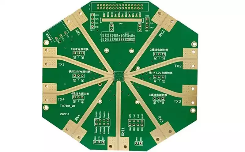
Product Name:Aluminum PCB
Material:aluminum base
Thickness: 1.0mm
Copper thickness: 1/OZ
Surface technology: OSP,HASL
Solder mask: White/Black/Red
Silk screen: White
Minimum line width/spacing: 35um
Minimum through-hole: 0.3mm
Application:LED
Copper pcb board,also known as metal substrate, is a special electronic material, is the most expensive and best thermal conductivity in the metal custody trips in one of the metal layer consists of high thermal conductivity of the copper plate, can carry a higher current, thermal conductivity is twice as much as the aluminium substrate, suitable for high-frequency circuits. High and low temperature changes in the application and the heat dissipation of precision communication equipment.
Copper pcb board circuit layer requires a large current-carrying capacity, and thus should use a thicker copper foil, the thickness of the general 35μm ~ 280μm. thermal conductivity insulating layer is the core technology of the copper substrate, the core thermal conductivity layer consists of aluminium trioxide and silica powder and epoxy resin-filled polymer composition, thermal resistance is small (0.15), visco-elastic performance is excellent, and has the ability to resist thermal aging, able to withstand mechanical and thermal stresses.
The heat dissipation principle of copper pcb board is to use the high thermal conductivity of copper, the heat generated by the electronic components quickly transferred to the copper substrate, and then through the heat sink and other heat dissipation devices will be emitted into the air, so as to achieve the purpose of cooling.
Copper pcb board is divided into gold-immersed copper substrate. Silver-plated copper substrate.Tin sprayed copper substrate. Antioxidant copper substrate. Copper substrate can be divided into: ordinary copper substrate and thermoelectric separation of copper substrate.The difference between them lies in the different thermal conductivity.
Ordinary copper pcb board
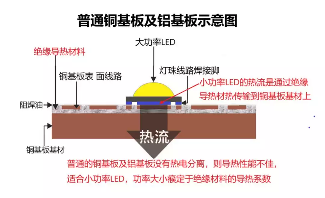
As shown in Figure 1, LED heat flow through the insulating thermal conductive materials to transfer heat to the copper substrate substrate, thermal conductivity depends on the thermal conductivity of the insulating materials, and insulating materials of the thermal conductivity is not too high, so the ordinary copper substrate is suitable for some small appliances with low power LED.

Figure 1 Ordinary copper pcb board
Thermoelectric separation of copper pcb board
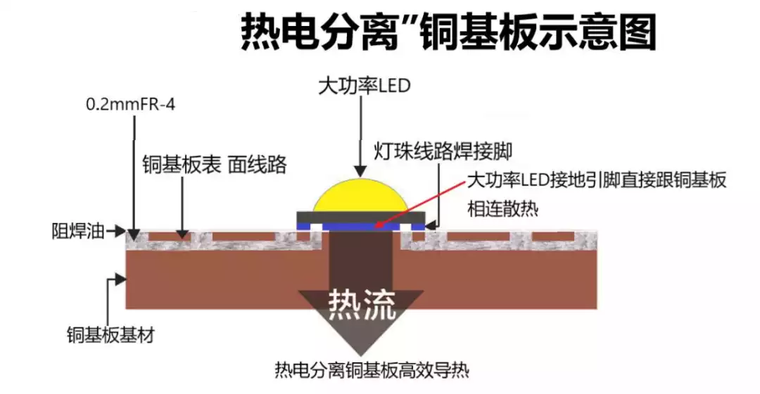
As shown in Figure 2, the ground pin of the LED is directly connected to the copper substrate to dissipate heat, thermoelectric separation of the copper substrate can be highly efficient thermal conductivity, so thermoelectric separation of the copper substrate is suitable for high-power automotive lamps LED beads.

Figure 2 Thermoelectric separation of copper pcb board
The circuit design part and the heat conduction part of the copper substrate are distributed in different circuit levels, and the heat conduction part is directly connected to the heat dissipation components of the LED beads, which achieves the optimal heat dissipation effect (i.e. no thermal resistance).
Thermally separated copper pcb has the following advantages:
1.The use of high-density copper as a substrate material makes the substrate itself has excellent heat carrying capacity and thermal conductivity and heat dissipation performance.
2.Through the design structure of thermoelectric separation, it achieves no thermal resistance contact with LED lamp beads, thus minimising the light decay of the lamp beads and prolonging their service life.
3.Due to the high density and strong thermal carrying capacity of the copper pcb, it can be designed to be smaller in size for the same power.
4.This substrate is very suitable for matching with individual high-power LED beads, especially those in COB package form, which can further enhance the overall effect of the lamps and lanterns.
5.According to the specific needs of customers, a variety of surface treatment (such as immersion gold, OSP, etc.), and the reliability of these surface treatment layers is extremely high.
6.In order to meet the design requirements of different lamps and lanterns, we can customise a variety of structures of thermoelectric separation of copper pcb (such as copper bump. Copper concave block. The thermal layer is parallel to the wiring layer, etc.).
However, thermoelectric separation of copper pcb board also has certain limitations: it is not suitable for single electrode chip bare crystal package.
The basic production process of copper pcb board:
1.Cutting:Cut the raw material of copper pcb boardinto the required size in production.
2.Drilling:Positioning holes are drilled into the copper pcb plate to provide assistance for subsequent processing.
3.Line imaging:in the copper pcb sheet material to present the line of the required part.
4.Etching:After the line is imaged, the required part is retained. The rest of the unwanted part of the etching off.
5.Screen Printing Solder Mask:Prevent non-soldering points from staining the solder, preventing tin from entering the short circuit. In the wave soldering solder resist layer is particularly important, can effectively prevent moisture and protect the circuit.
6.Silkscreen characters: for labelling.
7.Surface treatment:play a role in protecting the surface of the copper pcb.
8.CNC: the whole board for CNC operation.
9.Voltage test: test whether the line is working properly.
10.Packing and shipping: Copper pcb board to confirm that the packaging is complete and beautiful, the number is correct.

Product Name:Aluminum PCB
Material:aluminum base
Thickness: 1.0mm
Copper thickness: 1/OZ
Surface technology: OSP,HASL
Solder mask: White/Black/Red
Silk screen: White
Minimum line width/spacing: 35um
Minimum through-hole: 0.3mm
Application:LED
iPCB Corporation provides support for PCB Prototype and Electronic Manufacturing. You can request consultation or quotation for PCB, PCBA and ODM here, please contact email: sales@ipcb.com
We will respond very quickly.