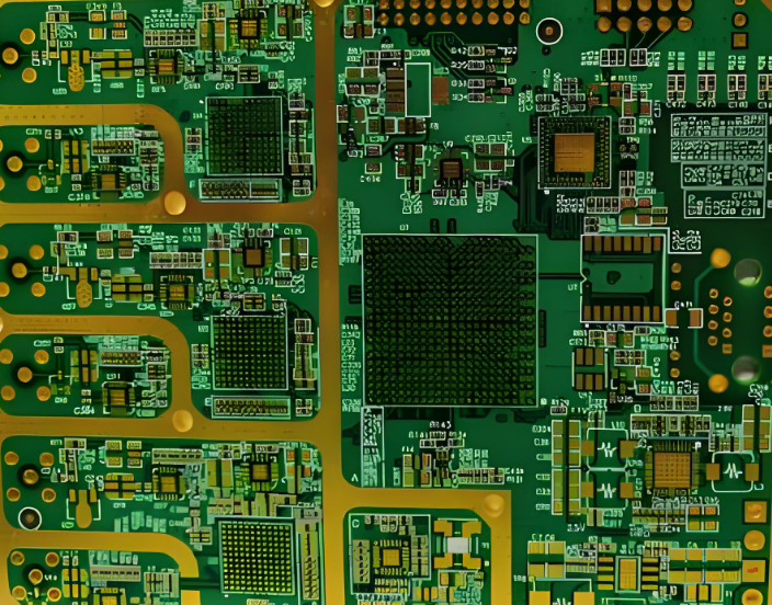
High-Density Interconnect printed circuit boards are crucial in modern electronics due to their efficient use of space and ability to accommodate complex circuitry. Within this category, buried vias and blind vias serve distinct purposes and exhibit unique characteristics. It's important to note that while most HDI PCBs incorporate blind vias, buried vias do not necessarily qualify as HDI unless specific design criteria are met.

HDI PCB
Understanding the Two Types of Vias
Blind Vias: Blind vias are holes that connect an outer layer of a PCB to one or more inner layers without extending completely through the board. These vias are beneficial for reducing layer count and improving signal integrity, particularly in multilayer designs. For instance, in a six-layer PCB, blind vias might connect layers 1-2 and 5-6, requiring laser drilling for fabrication.
Buried Vias: Buried vias, conversely, are entirely contained within the internal layers of a PCB, hidden from both the top and bottom surfaces. They interconnect inner layers, thus facilitating efficient routing without expanding the PCB's footprint. The application of buried vias is typically more complex and is used primarily in high-end designs where additional routing capacity is necessary.
Differences in HDI PCB Classification
6-Layer HDI PCB Classification:
First-Order HDI PCB: This configuration includes blind holes located between the 1st and 2nd layers (1-2) and the 5th and 6th layers (5-6). Both connections require laser drilling, confirming the board's status as a first-order HDI PCB.
Second-Order HDI PCB: Second-order HDI PCBs have an increased complexity with multiple blind holes that may involve various combinations of layers. For example:
The vias could connect 1-2, 2-3, 3-4, 4-5, and 5-6, requiring two separate laser drilling processes.
The production process for a second-order HDI PCB consists of drilling buried vias (3-4) first, followed by subsequent layers (2-5), with the final drilling occurring on the exterior connections (1-2, 5-6).
Second-order HDI boards can be further classified into two subcategories:
Second-Order HDI with Offset Vias: Blind holes such as 1-2 and 2-3 do not align.
Stacked Hole Design: Features overlapping vias like 1-3 and 3-4, indicating a more condensed inner structure.
Innovations and Evolving Techniques
The industry continues to see advancements in HDI PCB technology. Recent developments, such as the integration of automated laser drilling systems and improved material compositions, allow for finer vias and increased reliability. Moreover, manufacturers are employing advanced design software and simulation tools to predict and enhance the performance of HDI PCBs before production begins.
Furthermore, the growing demand for smaller electronic devices has accelerated the need for effective HDI designs, prompting an increased focus on making buried and blind vias more efficient. This includes research into new materials that can withstand tighter tolerances and increased thermal and electrical conductivity, catering to high-frequency applications.
Conclusion
In conclusion, understanding the distinctions between HDI buried and blind PCBs is essential for designers looking to optimize circuit board layouts for performance and reliability. While buried vias offer additional routing options within the confines of a PCB, blind vias are essential for maintaining signal integrity across multiple layers. As technology advances, the capabilities and designs of HDI PCBs will continue to evolve, meeting the demands of more intricate electronic systems.