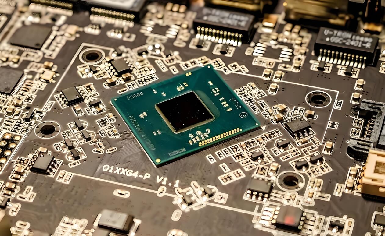
With the birth of PCBs in the 1950s, the technology has evolved rapidly, leading to a wide variety of types and applications. Among these, High-speed PCBs have emerged as a critical component for industries requiring advanced performance, such as telecommunications, satellites, and modern automobiles. As electronic devices become more precise and multifunctional, the demand for high-frequency, high-precision PCBs increases. These specialized boards require superior quality, advanced materials, and meticulous design to meet the rigorous standards of today's technological advancements.
What is a high-speed PCB?
Before talking about high-speed PCB design, we need to understand what a high-speed PCB is. Usually we call PCBs with signal transmission frequencies above 1GHz high-speed printed circuit boards. Unlike traditional PCBs, such PCBs have extremely high precision, technology, and material requirements. They are usually used in signal transmission products such as automobiles, radars, instruments, etc.
Especially with the emergence of 5G, the rapid development of RF components, the increasing demand for data processors, etc., electronic products have higher and higher requirements for data transmission and video processing.
The difference between high-speed PCBs and ordinary PCBs lies in four parameters: DK value, DF, water absorption, and impedance. DK and DF are essential for fast and stable transmission, while DF and water absorption affect the quality of signal transmission. Low water absorption reduces the DK and DF values, while strong water absorption increases the loss value. Low impedance ensures better signal transmission quality.
High-speed PCB Design Guidelines
The advancement of science and technology has led to increasing requirements for electronic devices, especially high-speed PCB design. This has increased the difficulty of design, and dense components, dense lines, and high-speed transmission components have become essential. Wiring is also an important link. The following is a guide to high-speed PCB design.
Number of layers
The first thing to confirm in high-speed PCB design is the number of PCB layers and size and whether BGA components are used. These are closely related to stacking and subsequent wiring. Confirming the size and number of layers of the PCB can also make it easier to confirm the stacking structure and preset line width. Secondly, the number of PCB layers will also directly affect the impedance of the stacking. Therefore, confirming the number of layers and size also indirectly affects the stacking. Since the development of high-speed PCB, it seems that the more layers, the higher the price.
According to design experience, some reservations will be made when designing high-speed PCBs, and relatively more layers will be used for design to avoid the need to add new layers when the function does not meet expectations after the design is completed, avoiding unnecessary problems.

High Speed PCB
Some rules and restrictions in high-speed PCB design
Before starting high-speed PCB design, signal line routing should be classified according to difficulty and importance. The higher the requirement, the higher the priority of the line must be, which is reflected in the width of the line and the number of tracks required to avoid line crossing, mutual interference and radiation effects.
Component layout
In the component layout in high-speed PCB design, the best situation is to modify the layout of some lines to achieve the best layout of the components. Attention should be paid to the number and area of the traces, including the wiring area. Generally speaking, too many vias will significantly increase the delay of the circuit. The best arrangement of the lines is to arrange them in parallel, avoiding line crossing and bending, so as to minimize the unfavorable factors such as mutual cross interference, reflected radiation, etc.
In particular, it is best to keep the two adjacent signals vertical as much as possible to prevent crossing and being too close, and further ensure the stability of signal transmission in high-speed PCB design.
Air outlet fan design
Usually, we connect each pin of the component to a via at this stage to achieve the internal connection of the PCB to achieve the former purpose. On the other hand, in order to improve efficiency, maximize the size of the circuit and vias as much as possible. In addition, the problem of high-speed PCB detection needs to be considered at this stage. In the high-speed PCB design guide, it is best to prepare the fixture in advance. This ensures that the board circuit is well detected. The fixture can be made at the same time as the PCB. So when the high-speed PCB is completed, the fixture progress is nearing the end, and then you can directly carry out 100% circuit testing.
Wiring layout
Finally, do a general check on the wiring on the high-speed PCB. If the line is too long, try to shorten the length of the line. In the final layout, pay attention to the design and adjust the unreasonable lines in the layout, which is the last step of the work. The above aspects are the normal high-speed PCB design guidelines we should follow.
In conclusion, high-speed PCB design requires careful attention to material selection, signal integrity, and layout practices to ensure optimal performance. By understanding the key factors and challenges, such as minimizing noise and managing power distribution, you can create more efficient and reliable PCBs. Whether you're designing for automotive, telecommunications, or any other high-speed application, the right approach to PCB design can make all the difference in the success of your project.