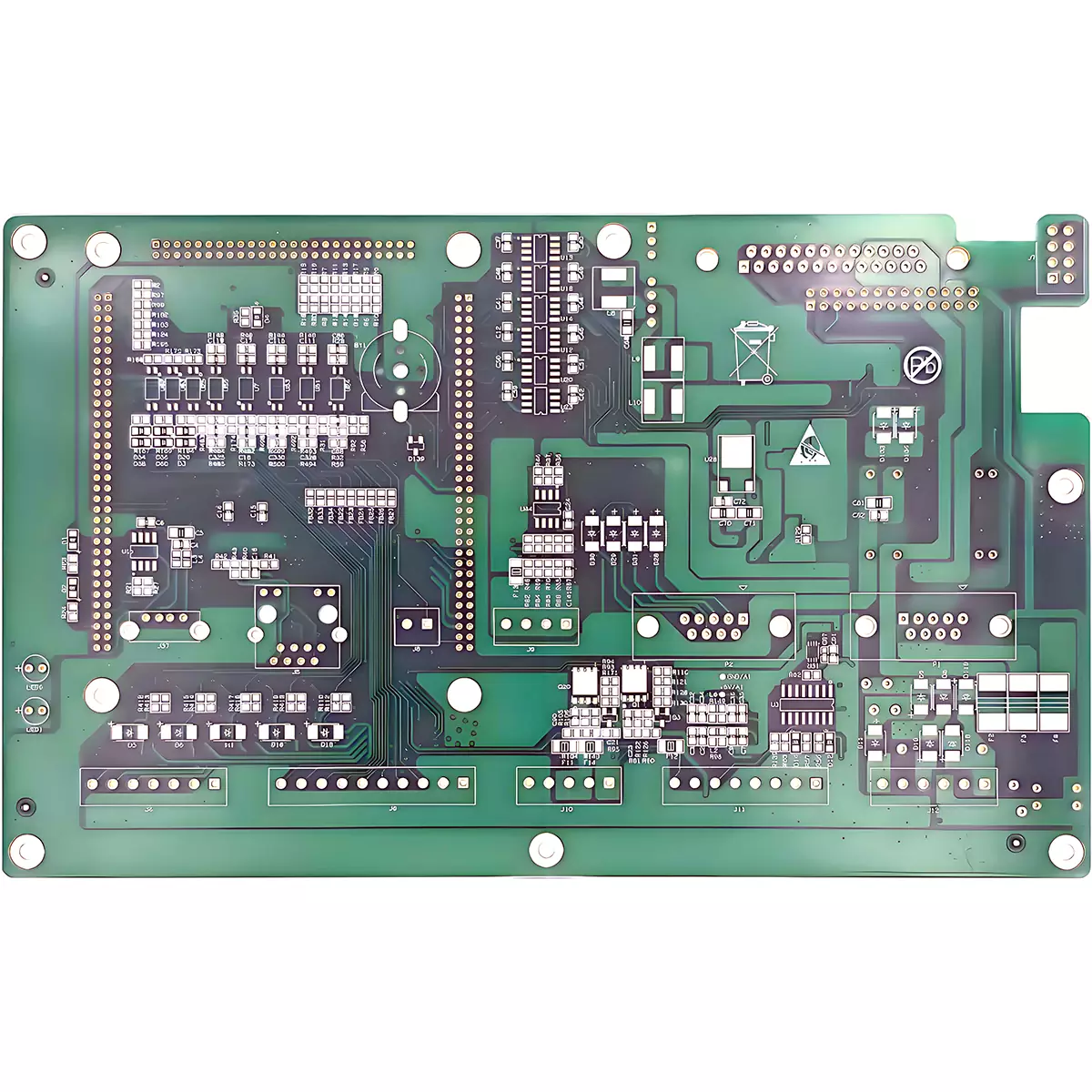
Product Name: Fiducial PCB
Material: KB-6061
Layers: 2Layers
Thickness: 1.6mm
Copper thickness: 1/1oz
Surface technology: HASL
Solder mask: Green
Silk screen: White
Minimum line width/spacing: 6/6mil
Minimum through-hole: 0.3mm
Application: Various electronic products
The reference point of Fidual PCB, also known as Mark point or Fidual mark, plays a crucial role in the assembly process. Fiducial PCB provides a common and measurable reference point for all assembly steps, ensuring that the equipment used for assembly can accurately locate the component packaging. In SMT production, the role of reference points is particularly significant. In short, if surface mount components are installed on the PCB circuit board, Mark points must be set up for the SMT machine to accurately locate them.
The reference point of Fiducial PCB is the basis for positioning the main components of the PCB by the placement machine. The shape, position design, and manufacturing accuracy of the reference point will directly affect the quality of the placement.
Fiducial PCB board come in Global Fiducial and Local Fiducial. Local Fiducial is typically used when components require high positional accuracy, such as high-density pin IC and BGA.
Multi panel Fiducial PCB include Panel Fiducial and Image Fiducial. Of course, Local Fiducial can also be placed in a PCB board.
The other requirements for Fiducial undoubtedly provide PCB design engineers with more design choices.
Solder pad Fiducial PCB design: The impact of solder pad design on the surface mount machine is mainly due to the position of the components on the PCB layout, which affects the suction nozzle of the mounting head. When laying out PCB components, design engineers should consider the minimum spacing between components relative to the difference in component thickness. The principle is to increase the spacing between components with large thickness differences as much as possible to avoid the suction nozzle touching thicker components during thin component mounting, resulting in lateral movement of thicker components and ultimately causing welding defects.
The PCB board edge distance from PCB components to the board feeding direction: Regarding the board transfer edge distance, there are two common standards in the SMT industry, namely 3mm edge distance and 5mm edge distance. Currently, 3mm edge distance is widely used, so PCB design engineers should pay special attention to using a minimum of 3mm edge distance, otherwise it will be limited during chip production.
When do I need Fiducial PCB markings?
Large scale assembly has always required Fidual PCB marking to ensure accurate placement and registration of parts. Small batch assembly, which you will see with prototypes or small batch experts, is not always necessary.
However, since there are small batch stores that rely entirely on them, you should inquire before making assumptions. Although PCB Fiducial marks may not be necessary for assembling any product, they are always a great idea and still work. When you can confirm that PCB reference marks are not needed, place these parts by hand.
However, since the replica of the circuit board is manufactured on the assembly line, it is necessary for the machine to understand the differences between the side and top/bottom of the circuit board. You wouldn't want your electronic devices to be placed in a way that follows no specific pattern.
What is the function of PCB reference marks?
In PCB design, the reference mark is a circular copper used as a reference point for picking up and placing the assembly machine. Fiducial PCB markings can help machines identify the orientation of PCB and their surface mount components, with packaging featuring tiny pitches such as quad planar packaging (QFP), ball grid arrays (BGAs), or quad planar no lead (QFN).
There are two common types of reference marks in printed circuit board design: global reference marks and local reference marks. The global reference mark is a copper reference placed at the edge of the PCB, allowing the machine to determine the direction of the board relative to the X-Y axis. The benchmark placement machine is also used to compensate for any tilt during PCB clamping.
The local reference mark is a copper mark placed outside the corner of the four package surface mount component. It is used by assembly machines to accurately locate the footprints of components and reduce errors in benchmark placement. This is particularly important when your design includes intricate tilts and large quad pack components.
Product Name: Fiducial PCB
Material: KB-6061
Layers: 2Layers
Thickness: 1.6mm
Copper thickness: 1/1oz
Surface technology: HASL
Solder mask: Green
Silk screen: White
Minimum line width/spacing: 6/6mil
Minimum through-hole: 0.3mm
Application: Various electronic products
iPCB Corporation provides support for PCB Prototype and Electronic Manufacturing. You can request consultation or quotation for PCB, PCBA and ODM here, please contact email: sales@ipcb.com
We will respond very quickly.