Share cost-effective products and high-quality services with customers. Contact Us


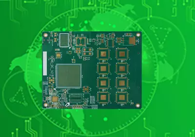
Knowing how to fix pcb board problems is important when electronic equipment stops working, develops intermittent faults, or shows visible signs of circuit damage. A printed circuit board can fail for many reasons, including damaged copper traces, short circuits, defective components, overheated solder joints, and corrosion caused by moisture or contamination. However, replacing components or applying solder without understanding the underlying fault can make the problem worse. Effective PCB repair begins with identifying the failure, determining its cause, and selecting a repair method that restores both electrical function and mechanical reliability.
PCB repair can range from a simple solder joint correction to a more complicated reconstruction of damaged conductive paths. The appropriate approach depends on the board's construction, the location and extent of the damage, component density, and the electrical requirements of the circuit. A small repair on an accessible single-sided board may be relatively straightforward, while damage to an internal layer of a multilayer PCB can be much more difficult to address.
Identify the Cause Before Repairing a PCB Board
The first step in PCB repair is a careful inspection. Before applying power or removing components, technicians should examine the board for discoloration, burnt areas, cracked components, lifted pads, damaged connectors, corrosion, and unusual solder joints. A magnifying tool or inspection microscope can help reveal fine cracks and defects that are difficult to see with the naked eye.
Visual inspection provides useful clues, but it cannot identify every electrical fault. A board may look normal while containing an open circuit, an unintended connection between copper traces, or a component that no longer operates within its specified range. Electrical measurements are therefore necessary to narrow down the cause.
A digital multimeter is one of the most useful tools for basic PCB troubleshooting. Continuity mode can help determine whether a trace or connection is broken, while resistance measurements can identify unexpected paths between circuit points. Voltage measurements, when performed under appropriate operating conditions, can help locate missing supply rails or abnormal voltage levels. Technicians should interpret these readings in the context of the circuit because capacitors, semiconductor junctions, and parallel components can affect measurement results.
Short circuits and open circuits are two common PCB faults. A short circuit occurs when conductive paths that should remain electrically separate become connected, potentially causing excessive current or preventing the circuit from starting. An open circuit occurs when an intended electrical path is interrupted, often because of a cracked trace, damaged via, failed solder joint, or disconnected component terminal. Identifying which type of fault is present helps determine where further testing should focus.
Component failure is another frequent cause of malfunction. Resistors may become damaged by excessive power dissipation, capacitors can lose their electrical characteristics or develop internal faults, and semiconductor devices may fail because of overvoltage, overheating, or electrostatic discharge. Replacing a component without checking the surrounding circuit can lead to repeated failure if the original cause remains unresolved.
Repair Common PCB Damage
When a copper trace is broken, the repair method depends on its width, location, and electrical function. For a simple accessible trace, a technician may remove damaged coating, clean the exposed copper, and restore the connection using an appropriately sized conductor or copper repair material. The repaired path must have suitable conductivity and mechanical stability. Afterward, the exposed area should be protected with an appropriate insulating coating to reduce the risk of corrosion or accidental contact.
Damaged solder joints require a different approach. A joint may become cracked after repeated thermal cycling, mechanical vibration, or poor soldering during assembly. The technician can remove defective solder, clean the pad and component terminal, and resolder the connection using a suitable process. However, if the pad has lifted from the substrate or the surrounding laminate is damaged, simply adding more solder will not provide a reliable repair.
Component replacement is necessary when testing confirms that an electronic part is defective. The replacement should match the original component's electrical specifications, package type, polarity, and relevant thermal characteristics. Before installing the new part, the technician should inspect the pads and surrounding circuitry for heat damage or contamination. Excessive heating during removal or installation can damage nearby components, weaken pads, or affect multilayer connections.
Corrosion caused by moisture or chemical contamination may also require attention. Contamination can create conductive paths between adjacent features, interfere with solderability, and gradually damage copper surfaces. The cleaning method must be compatible with the board materials and components. After cleaning, the board should be dried appropriately and inspected to confirm that residues and damaged areas have been addressed.
Not all damage can be repaired economically or safely. A multilayer PCB with a damaged internal power plane, severely burnt laminate, or extensive delamination may require specialized reconstruction or complete replacement. If the damage affects safety-critical circuitry, high-voltage sections, or controlled-impedance signal paths, repair should only proceed when the original electrical and safety requirements can be verified.
Tools and Precautions for PCB Repair
Successful PCB repair depends on using suitable tools and controlling the repair environment. A temperature-controlled soldering station helps maintain consistent heating, while appropriate solder, flux, tweezers, wire cutters, and desoldering equipment support accurate work. A multimeter is essential for basic electrical verification, and an inspection microscope can improve accuracy when dealing with fine-pitch components or narrow copper traces.
Electrostatic discharge protection is particularly important when handling sensitive integrated circuits and semiconductor components. A grounded ESD workstation, suitable wrist strap, and antistatic handling practices can reduce the risk of damaging components during inspection and repair. The board should also be disconnected from its power source before resistance or continuity measurements are performed. Capacitors may retain stored energy after power is removed, so appropriate discharge and verification procedures are necessary before working on the circuit.
Thermal control is equally important. Applying excessive heat for too long can lift copper pads, damage the substrate, weaken nearby solder joints, or cause internal delamination. The repair process should use a temperature and heating duration appropriate for the solder alloy, component package, and board construction. For complex assemblies, specialized rework equipment may be necessary to control heating across multiple terminals.
Technicians should also consider the original purpose of the board. A repair that restores basic continuity may not be sufficient for a high-speed communication circuit, RF module, or precision measurement system. Changes to trace geometry, grounding, shielding, or component placement can affect electrical performance even when the circuit appears to function.
Verify the PCB Board After Repair
A repaired board should never be considered reliable based solely on its appearance. After the repair, technicians should inspect the affected area for solder bridges, loose wires, damaged insulation, incomplete joints, and remaining contamination. Continuity testing can confirm that repaired connections are electrically complete, while resistance checks can help identify unintended shorts between adjacent nets.
The next step is to verify the relevant power and signal conditions. Supply voltages should be checked against the circuit requirements, and key signals should be measured where suitable test points are available. For more complex circuits, an oscilloscope or specialized test equipment may be needed to evaluate waveform quality, timing, noise, or other performance characteristics.
Functional testing should follow once basic electrical checks have been completed. The board can be operated under controlled conditions to confirm that the original function has been restored. Depending on the application, additional thermal observation, load testing, or environmental testing may be appropriate. These checks help reveal intermittent problems that might not appear during a brief power-on test.
The repair should also be documented, especially when the PCB board is part of industrial equipment or a product with maintenance requirements. Recording the original fault, damaged area, components replaced, repair method, and verification results makes future troubleshooting easier and helps determine whether the board is suitable for continued service.
Ultimately, the best way to fix pcb board problems is to combine accurate fault diagnosis with a repair method suited to the board's construction and operating requirements. Correcting the visible damage is only one part of the process; the repaired circuit must also pass electrical and functional checks. When the damage is extensive or involves complex internal structures, professional PCB repair or replacement may provide a more dependable solution than an improvised repair.
