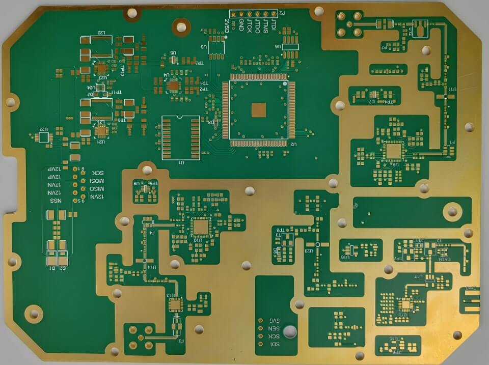
Routing is a critical step in PCB design, often regarded as the culmination of previous preparatory work. It requires the highest level of precision and effort. PCB routing can be single-sided, double-sided, or multilayered, employing either automated or interactive methods. Prior to automated routing, interactive techniques should be used for stringent connections. Input and output lines should avoid parallel adjacency to prevent reflection interference, and ground isolation should be added as necessary. Adjacent layer routing should be perpendicular to minimize parasitic coupling.
The success of automated routing relies on good layout practices, with predefined routing rules that encompass bend limits, via counts, and step numbers. Typically, routing begins with exploratory connections to quickly establish short paths, followed by maze-like routing for global optimization. This may involve disconnecting and rerouting established paths for improved outcomes.
In high-density PCB designs, traditional vias can be inadequate, leading to the adoption of blind and buried vias, which not only serve as connections but also free up routing space, enhancing overall routing efficiency. Mastering PCB design is a nuanced process that requires experience and understanding from engineers.

PCB Design
1. Handling Power and Ground Lines
Even if routing is well-executed, inadequate power and ground line management can degrade product performance. Thus, minimizing noise interference from power and ground lines is essential for product quality. Engineers must understand the noise generation between these lines and implement noise suppression techniques such as decoupling capacitors and wider traces, ensuring ground lines are wider than power lines. Digital circuits may utilize wide ground traces to form a ground plane, which is not suitable for analog circuits.
2. Common Ground Handling in Digital and Analog Circuits
Many PCBs now integrate both digital and analog circuits, necessitating careful consideration of interference, especially noise on ground lines. High-frequency digital signals should be kept away from sensitive analog components, and a common grounding scheme must be implemented within the PCB to isolate digital and analog grounds, only connecting them at a single point externally.
3. Signal Lines on Power (Ground) Layers
In multilayer PCBs, if signal layers are nearly full, routing on power or ground layers can be a viable solution. Power layers should be prioritized for routing before using ground layers to maintain their integrity.
4. Connection Pad Management in Large Conductors
When connecting component pads to large ground areas, electrical performance is paramount. Ideally, pads should fully contact the copper plane, but this can lead to soldering challenges. A cross-shaped pad design, known as a thermal pad, can mitigate heat dispersion during soldering, reducing the risk of cold joints.
5. The Role of Network Systems in Routing
In many CAD systems, routing decisions rely on network systems. An overly dense grid increases pathway options but can overload memory and computational resources, while a sparse grid severely limits routing efficiency. A balanced grid system is crucial for effective routing.
6. Design Rule Check (DRC)
After completing the routing design, it is vital to verify compliance with established design rules and production requirements. This includes checking distances between lines, pad dimensions, coupling between power and ground lines, and ensuring independent ground lines for analog and digital circuits. Additional considerations involve verifying the placement of graphics on the PCB and ensuring adequate process lines.
This comprehensive approach to PCB design is essential for achieving high-quality, reliable electronic products.