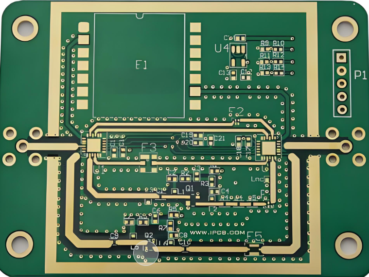
High-Frequency PCB Layout
The continuous advancement of digital components has led to designs that prioritize high speed, low power consumption, compact size, and enhanced resistance to electromagnetic interference . These developments necessitate a re-evaluation of printed circuit board (PCB) design and layout techniques, especially for High-frequency PCBs. Below are key recommendations reflecting the latest standards and technologies in the industry.

RF-PCB
1. Embrace Multilayer Structures
Modern High-frequency circuits are characterized by high integration density. Multi-layer PCB designs are crucial for minimizing interference and preserving signal integrity. These boards typically incorporate dedicated layers for power and ground routing, significantly reducing the risks of crosstalk and electromagnetic compatibility issues.
2. Optimize Routing Techniques
When designing high-speed circuits, aim to minimize circuit bends and keep routing as linear as possible. Utilizing straight traces is preferred, but if turns are necessary, 45-degree angles or gentle curves should be used. Implementing advanced routing technologies, such as differential pair routing, can further enhance signal performance.
3. Implement Short Traces
Keeping circuit traces short between components is vital for maintaining signal quality and reducing parasitic inductance and capacitance. This approach is essential in high-frequency PCBs where every millimeter can affect performance.
4. Minimize Layer Changes
Reduce the number of vias and transitions between layers during layout. Each via can introduce up to 0.5 pF of stray capacitance. By minimizing these transitions, designers can improve signal integrity and reduce the potential for signal loss, particularly in high-speed data transmission circuits.
5. Address Parallel Line Interference
To tackle staggered interference from parallel signal lines, consider implementing ground planes on adjacent layers. Techniques such as using guard traces or ground reference traces can also help mitigate unwanted coupling effects. For multilayer designs, ensure orthogonal routing between layers to further reduce interference.
6. Advanced Grounding Techniques
Utilizing a solid ground plane is critical, particularly for high-frequency designs. Grounding techniques should include star grounding or ground fill to help reduce return path inductance and improve overall system stability. Additionally, consider integrating a ground bounce analysis during simulation.
7. Avoid Current Loops
Ensure that no loops are formed in signal traces, as this can lead to increased EMI. Proper grounding practices are essential to prevent the formation of ground loops and ensure clean signal operation.
8. Integrate Decoupling Capacitors Effectively
Position high-frequency decoupling capacitors as close as possible to each integrated circuit (IC) to filter out power supply noise. Utilizing high-quality ceramic capacitors with low equivalent series resistance can significantly enhance performance.
9. Utilize Choke Links for Ground Connections
When connecting analog and digital ground planes, incorporate choke links or ferrite beads to filter out high-frequency noise. While such components are often omitted from circuit schematics, their implementation in layouts is crucial to ensure effective grounding without degrading performance.
10. Isolate Digital and Analog Blocks
Separating digital and analog circuits is vital to reduce mutual interference. Ensure that the power and ground connections of each block converge at a single point to prevent noise coupling between analog and digital domains.
11. Filter Power Supply Inputs
For components like DSPs, integrating filter capacitors as close as possible to their power pins is essential to suppress power supply noise. Employing ferrite beads or LC filters can also enhance power integrity by filtering unwanted high-frequency signals.
12. Optimize Memory Placement and Access Speed
Place off-chip memory modules as close as possible to DSPs, maintaining equal lengths for data, address, and control lines to minimize timing discrepancies. In systems involving multiple memories, consider using memory controllers with matching access speeds to the DSP, ensuring efficient data handling.
13. Harness Advanced PCB Simulation and Design Tools
With the rise of sophisticated simulation platforms, designers are encouraged to utilize tools such as finite element analysis (FEA) and electromagnetic simulation software. These tools can provide insights into potential issues, such as crosstalk and impedance mismatches, before production. Implementing simulation in the design phase is vital for ensuring the reliability and performance of high-frequency circuit boards.
Conclusion:
Incorporating these best practices will empower PCB designers to create high-frequency circuit boards that perform reliably and effectively in various applications. The ongoing evolution of technologies demands that designers stay updated on the latest techniques and tools to maintain competitive edges and optimize product performance.