Share cost-effective products and high-quality services with customers. Contact Us


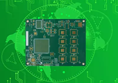
What Is Circuit Board Shielding?Circuit board shielding is the use of conductive or specially designed structures to limit electromagnetic interference on or around a printed circuit board. The basic purpose is to control the movement of unwanted electromagnetic energy between different parts of an electronic system.
There are two common objectives. The first is to prevent electromagnetic energy generated by a circuit from reaching other circuits or escaping from the product. The second is to protect sensitive circuitry from electromagnetic energy generated elsewhere. In many electronic devices, both functions are important.
For example, an RF transmitter can generate electromagnetic energy that affects a nearby receiver or sensitive analog circuit. A high-speed processor can produce fast signal transitions that couple into neighboring traces, while a switching power supply can generate broadband noise through both conducted and radiated paths.
A shielding structure creates a controlled boundary around the affected circuit. When it is properly connected to the ground structure and integrated with the PCB layout, it can reduce the amount of electromagnetic energy that crosses this boundary.
The effectiveness of electromagnetic shielding depends on several factors, including frequency, material properties, geometry, electrical continuity, grounding, and the size and location of openings in the shielding structure.
Why Does a PCB Need Shielding?
Not every PCB requires a dedicated shielding structure. In many applications, careful PCB layout, grounding, filtering, and component placement can reduce EMI to an acceptable level without adding a separate metal enclosure.
Circuit board shielding becomes more useful when a design contains strong noise sources or highly sensitive circuits that are difficult to isolate through layout alone. Common examples include RF communication circuits, wireless modules, sensitive analog front ends, clock generators, high-speed digital circuits, and switching power supplies.
Mixed-signal boards can also benefit from additional shielding when noisy digital or power circuits operate close to sensitive analog or RF sections. Physical isolation can become particularly important when limited board space prevents designers from achieving sufficient separation through component placement.
There are two basic reasons to use EMI shielding on a circuit board. The first is emission control, which limits unwanted electromagnetic energy generated by the PCB from affecting nearby circuits or external equipment. The second is immunity improvement, which protects sensitive circuitry from external electromagnetic interference.
This means shielding is not simply about preventing a PCB from producing noise. It can also help prevent sensitive circuits from receiving unwanted noise.
How Does Circuit Board Shielding Work?
A conductive shield changes the electromagnetic environment around a circuit. When electromagnetic energy reaches a conductive shielding structure, part of the energy can be reflected while another portion can be absorbed by the material. The actual shielding performance depends on the frequency, material, geometry, thickness, field type, and overall structure.
For PCB applications, the physical shield itself is only one part of the system. Its electrical connection to the intended ground structure is equally important. The ground plane, vias, shield perimeter, component placement, and surrounding enclosure can all influence the final result.
A metal cover placed over a noisy circuit does not automatically provide effective EMI protection. Poor grounding, large openings, discontinuities, and unsuitable mechanical geometry can allow electromagnetic energy to couple through the structure.
The same principle applies to traces and vias. A connection that appears electrically continuous at low frequencies may behave differently at higher frequencies because inductance and parasitic effects become increasingly important.
This is why effective Circuit Board Shielding needs to be designed according to the frequency range and coupling mechanism rather than simply adding conductive material around a circuit.
Common Circuit Board Shielding Methods
Several methods can be used to control electromagnetic interference on a PCB. The appropriate approach depends on the operating frequency, circuit architecture, available board space, mechanical design, thermal requirements, manufacturing process, and required level of isolation.
Ground Planes
A continuous ground plane is one of the fundamental structures used for controlling electromagnetic behavior on a circuit board.
A solid reference plane provides a low-impedance return path for many signals and helps reduce current loop areas. It can also reduce unwanted coupling between different areas of the PCB when the signal and return paths are properly designed.
However, a ground plane should not be considered a complete replacement for other shielding techniques. Poor routing, plane discontinuities, inappropriate return paths, and badly positioned high-speed signals can still create EMI problems.
For this reason, grounding and circuit board shielding should be considered together during PCB layout.
Via Stitching and Via Fences
Via stitching connects copper regions on different PCB layers through multiple vias. When a series of grounded vias is arranged around a circuit or along a board boundary, the structure is commonly known as a via fence.
Via fences can help control electromagnetic coupling between different PCB regions. They are particularly useful around RF circuits, transmission lines, board edges, and other areas where electrical isolation is important.
The spacing between vias is an important design consideration because shielding performance changes with frequency. A commonly used engineering guideline is to keep via spacing substantially smaller than the wavelength of the highest frequency of concern, with λ/20 sometimes used as a starting point.
This should not be treated as a universal design requirement. The appropriate spacing depends on the actual PCB structure, frequency range, board thickness, manufacturing capability, and EMC objectives.
Copper Guard Structures
Grounded copper pours and guard areas can provide additional isolation between different circuit sections.
For example, a sensitive analog circuit can be surrounded by a grounded copper region to reduce coupling from nearby digital or RF circuitry. The effectiveness of this approach depends heavily on how the guard structure is connected to the overall ground system and how return currents flow through the PCB.
A copper guard should therefore be treated as part of the complete grounding and PCB shielding strategy rather than as an isolated copper feature.
Metal Shielding Cans
A metal shielding can is a conductive enclosure mounted directly onto the PCB around a selected circuit or group of components.
Instead of shielding the entire board, the enclosure covers only the circuit that requires additional protection. This makes localized EMI shielding useful when a PCB contains several functional blocks with different electromagnetic characteristics.
For example, a metal shield can cover an RF section while the remaining areas of the circuit board remain exposed. This creates a localized electromagnetic barrier without requiring the entire PCB to be enclosed.
The shielding footprint, component height, grounding points, soldering process, thermal conditions, and access for inspection or repair should all be considered during PCB design.
Shielding Between Circuit Sections
Some circuit boards contain multiple functional blocks that operate at very different frequencies or have very different noise characteristics.
A digital processor, switching regulator, RF transmitter, and sensitive analog amplifier may all share the same PCB. Simply increasing the distance between these circuits may not provide enough isolation, particularly when the board has strict size limitations.
Designers can combine grounded structures, via fences, controlled routing, filtering, and localized shielding to create greater separation between functional blocks.
This approach is especially useful in mixed-signal and RF designs where unwanted electromagnetic coupling can affect signal integrity, receiver sensitivity, or overall EMC performance.
Circuit Board Shielding Design Considerations
Effective circuit board shielding depends on much more than the choice of conductive material. The electrical, mechanical, thermal, and manufacturing aspects of the design should be considered together.
Ground Connection
A shielding structure needs an appropriate electrical connection to the intended reference or ground structure.
A poor connection can introduce impedance into the shielding path and reduce its effectiveness. At higher frequencies, even a connection that appears electrically short can have significant inductance.
For this reason, shield connections are generally designed with short, low-impedance paths and sufficient connection points around the shield perimeter.
The relationship between the shield, PCB ground plane, chassis, and other grounding structures should also be considered as part of the complete EMC design.
Openings and Gaps
Openings in a shield can become leakage paths for electromagnetic energy.
Ventilation holes, connector openings, seams, component access areas, and gaps between shielding structures can all influence shielding performance. As frequency increases, relatively small openings can become more significant because the corresponding wavelength becomes shorter.
A shielding structure should therefore be evaluated as a complete enclosure rather than simply as a conductive surface.
Via Spacing
Via fences are effective only when their spacing is appropriate for the frequency being controlled.
A fence with widely spaced vias may provide limited isolation at higher frequencies because electromagnetic energy can couple through the spaces between adjacent vias. Tighter spacing can improve the electrical continuity of the shielding boundary, although the optimum design also depends on board thickness, PCB geometry, manufacturing tolerances, and the target frequency range.
The goal is not simply to use as many vias as possible. The spacing should be selected according to the electrical requirements and manufacturing constraints of the design.
Shield Height and Component Placement
When a metal shield is used, all components underneath it must fit within the available internal height.
This requirement affects component selection, placement, routing, thermal management, and mechanical design. If shielding is added late in the development process, existing components may need to be moved or replaced.
Integrating the shielding structure during PCB layout makes it easier to maintain the required electrical clearance, mechanical dimensions, and component accessibility.
Thermal Management
A shield can change the thermal environment around the components it covers.
High-power devices may require additional heat spreading or a different mechanical structure. A fully enclosed area can also make heat dissipation more difficult when several active components operate beneath the same shield.
Electrical shielding and thermal management should therefore be evaluated together, especially in compact electronic products.
Manufacturing and Assembly
The shielding structure must also be compatible with the PCB manufacturing and assembly process.
The PCB footprint needs suitable solderable areas and adequate clearances. Shielding structures can affect solder paste printing, component placement, reflow, inspection, repair, and maintenance.
For volume production, mechanical tolerances between the PCB and shield should be considered at the same time as electrical requirements. Designing the shielding structure early can reduce the risk of manufacturing changes later in the project.
When Should You Use Circuit Board Shielding?
Circuit board shielding is generally considered when a PCB has an EMI or EMC problem that cannot be adequately controlled through layout, grounding, filtering, and other design measures, or when the circuit architecture requires physical isolation from the beginning.
A shielding structure may be useful when an RF circuit is located close to sensitive analog electronics, when high-speed circuitry generates unwanted radiation, when a noisy power section is close to a sensitive circuit, or when external electromagnetic fields can affect critical circuitry.
It can also be useful when several functional blocks need to coexist within a small PCB area and there is insufficient physical space to achieve adequate isolation through component placement alone.
However, adding a shield should not automatically be the first response to an EMI problem. PCB layout, grounding, signal return paths, decoupling, filtering, and power distribution should be examined first.
The actual coupling path should be identified before selecting a shielding method. If interference is primarily conducted through a power supply, ground connection, connector, or cable, placing a metal shield over the PCB may not address the underlying problem.
Circuit Board Shielding vs PCB Layout Control
Circuit board shielding and PCB layout control address related but different aspects of electromagnetic compatibility.
PCB layout attempts to reduce unwanted electromagnetic coupling at its source. Good component placement, short current loops, appropriate return paths, controlled impedance, proper grounding, and suitable separation between noisy and sensitive circuits can all reduce the generation and propagation of interference.
Shielding provides an additional physical barrier when these measures are not sufficient.
This distinction is important because a poorly designed PCB can still have EMI problems after a shield is installed. If the interference travels through a power line, ground connection, connector, or external cable, a metal enclosure around one circuit may have limited impact.
Effective EMI control therefore starts with understanding where the interference originates and how it reaches the affected circuit. The shielding method can then be selected according to the actual coupling mechanism.
How to Improve Circuit Board Shielding
A reliable approach is to treat shielding as part of the PCB architecture rather than as an isolated component added near the end of development.
The process should begin by identifying the main noise sources and the circuits most vulnerable to interference. The next step is to determine how electromagnetic energy is coupling between them. The coupling path may involve PCB traces, power planes, ground structures, cables, connectors, board edges, or free-space radiation.
Once the coupling mechanism is understood, the PCB can be designed with appropriate grounding, routing, return paths, via stitching, copper isolation, filtering, and physical shielding.
For a sensitive RF or mixed-signal section, a combination of a controlled ground structure, short return paths, appropriate via stitching, and a local shield can provide greater isolation than relying on a shield alone.
The final design should be evaluated through simulation, pre-compliance testing, or laboratory EMC testing as appropriate for the product and applicable requirements.
Circuit board shielding is an important technique for controlling electromagnetic interference on a PCB. It can protect sensitive circuits from external electromagnetic energy while also limiting unwanted emissions from noisy circuit sections.Common approaches include ground planes, copper isolation structures, via fences, and localized metal shielding. Their effectiveness depends on frequency, geometry, grounding, openings, material properties, component placement, and the overall PCB architecture.
