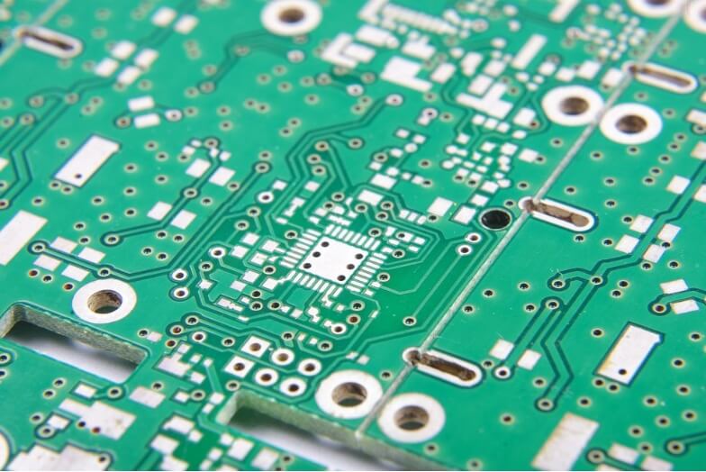
In PCB (Printed Circuit Board) design, the processing of power ground and signal ground is a key step to ensure circuit stability and reliability. The following are detailed suggestions for power ground and signal ground processing:
1. Power ground processing
Heat dissipation design:
Power devices generate a lot of heat when working, so thermal management is the primary task of power PCB design. It is necessary to design appropriate heat dissipation structures, such as heat sinks, heat pipes, etc., to improve the heat conduction efficiency.
Increase the copper foil area of PCB to improve heat conduction capacity while reducing the resistance of copper foil.
Power path optimization:
Optimize the power path and reduce the resistance and inductance on the power line to reduce voltage drop and ripple. The power line should be wide enough to provide sufficient current transmission capacity, and try to keep the wiring direct and short.
Decoupling capacitor:
Place appropriate decoupling capacitors on the power line to filter out high-frequency noise. The decoupling capacitor should be close to the power access point of the power device to reduce the lead inductance.
Multilayer board design:
In multilayer board design, use dedicated power layers and ground layers to improve the stability of the power supply. Power components should be close to the corresponding power and ground connection points to reduce the resistance on the path.
Single-point grounding: For low-frequency circuits, single-point grounding can be used to connect the power ground and the ground of other parts at one point to reduce the difference in ground voltage.

PCB
2. Signal ground processing
Separate ground plane:
Divide the ground line into two areas, analog ground and digital ground, and use two independent ground planes for routing. This can prevent mutual interference between analog and digital signals. The distance between analog ground and digital ground should be appropriate, and it is generally recommended to be no less than 1mm, but the specific distance needs to be adjusted according to circuit characteristics and structural limitations.
Use copper plating and shielding:
Lay copper foil on the ground area of the circuit board to form a ground plane to reduce the resistance and inductance of the ground line and improve the working stability and anti-interference ability of the circuit. The use of shielding can also isolate the ground line and power line to a certain extent, reducing interference and electromagnetic radiation.
Good grounding layout:
The selection and layout of the grounding point are very important. Low-impedance and low-noise grounding points should be selected, and the grounding point should be placed in the center of the circuit as much as possible for easy routing.
Differential routing:
For differential signals, the length, width and spacing of the differential routing should be kept consistent to reduce differential imbalance and interference.
Separation of power supply and signal:
When laying out, the power line and signal line should be separated as much as possible to avoid interference between them. Especially for noise-sensitive circuits, more stringent separation measures should be taken.
3. Comprehensive processing
Simulation analysis:
Perform thermal simulation, electromagnetic compatibility simulation and signal integrity simulation in the design stage to predict and optimize the performance of the circuit.
Prototype testing:
Make a prototype and perform actual testing to verify whether the design meets the requirements. Through testing, potential problems can be discovered and the design can be optimized.
Design documentation:
Record the design process and decisions in detail to facilitate team communication and subsequent maintenance. Provide clear annotations in the PCB layout, including component values, reference numbers, and direction indications.
In summary, the processing of Power ground and Signal ground needs to comprehensively consider heat dissipation, power path, decoupling capacitors, multi-layer board design, single-point grounding, separate ground planes, copper plating and shielding, etc. Through reasonable design and optimization, the stability and reliability of PCB can be ensured.