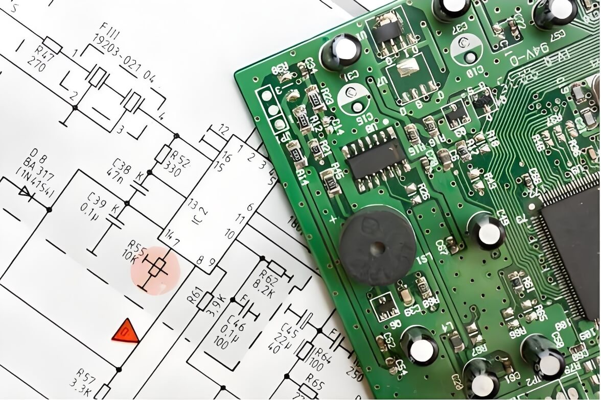
In Altium Designer (AD for short), associating the schematic with the PCB is an important design step that ensures a smooth transition from logical design to physical implementation.
The following are the steps to associate the schematic and PCB:
1. Distribution component packaging
Check and assign encapsulation:
In the schematic, each component needs to have a corresponding PCB package to represent its physical form and pin layout in the PCB design.
Check that each component in the schematic has been assigned the correct footprint. If not, you need to assign a footprint to the component through the library manager or directly from
the component library.
Ensure packaging consistency:
Make sure that the component package in the schematic is completely consistent with the package used in the PCB design, including the number of pins, pin spacing, package size, etc.
2. Update PCB documentation
Perform update operation:
In the schematic editor, click the Design option on the menu bar and select Update PCB Document or similar option.
In the pop-up dialog box, select the PCB file to be updated and click the "Execute Changes" button.
Observe the import results:
AD will try to synchronize the components and connection information in the schematic to the PCB file. After the import is complete, the results can be viewed in the PCB Editor.
3. Interactive layout and routing
Use interactive layout features:
AD provides an interactive layout feature that allows users to view the schematic and PCB layout simultaneously and interact between the two views.
By placing the schematic and PCB in two windows and setting the interaction mode, when you click on a component in the schematic, the corresponding component and connection will be
highlighted in the PCB view.
Auxiliary wiring:
In interactive layout mode, users can more intuitively understand the connection relationships between components and perform routing accordingly.
Use the wiring tools provided by AD to conduct wiring according to the design rules to ensure signal integrity and electromagnetic compatibility.

Schematic Diagram
4. Inspection and Optimization
DRC check:
After completing the wiring, perform a DRC (Design Rule Check) check to verify whether the PCB design meets all design rule requirements.
Make necessary corrections and optimizations based on the DRC inspection results.
Optimize layout and routing:
Optimize PCB layout and wiring based on DRC inspection results and actual needs.
Adjust component positions, rotation angles, and routing paths to improve circuit performance and reliability.
5. Precautions
Ensure software version compatibility:
When doing schematic and PCB design, make sure that the AD software versions you use are compatible with each other.
Follow design specifications:
During the design process, please follow relevant design specifications and standards to ensure the correctness and reliability of the design.
Back up important files:
Before performing important operations, be sure to back up the schematic and PCB files to prevent data loss or damage.
Through the above steps and precautions, you can successfully associate the Schematic Diagram and PCB in AD and achieve a smooth transition from logical design to
physical implementation.