Share cost-effective products and high-quality services with customers. Contact Us


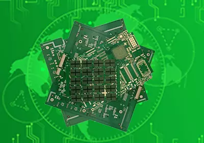
Making a multilayer PCB is a controlled manufacturing process that combines several patterned copper layers with insulating dielectric materials to form a single circuit board. Unlike a single-sided or double-sided PCB, a multilayer board contains internal copper layers that cannot be accessed once the board has been laminated. This makes layer alignment, material selection, lamination, drilling, plating, and inspection particularly important.
A typical multilayer PCB may contain four, six, eight, or more copper layers. Some advanced designs can contain many more layers when the circuit requires additional routing capacity, controlled impedance, power distribution, or a higher level of integration. The basic manufacturing principle remains the same: individual inner layers are fabricated first, the layers are accurately stacked and laminated, and the finished structure is then drilled, plated, patterned, finished, and electrically tested.
Understanding how a multilayer PCB is made is useful not only for manufacturing engineers. PCB designers and purchasing teams can also benefit from understanding the process because many manufacturing problems can be prevented before production begins.
How Is a Multilayer PCB Made?
The multilayer PCB manufacturing process begins with engineering preparation and ends with electrical testing and final inspection. Although the exact sequence varies depending on the PCB structure and manufacturing technology, a conventional rigid multilayer PCB generally follows this route:
Design and DFM review → inner layer fabrication → inner layer inspection → stack-up and lamination → drilling → hole preparation and copper plating → outer layer fabrication → solder mask and surface finish → profiling → electrical testing and final inspection
For a standard multilayer PCB with plated through-holes, this workflow provides the basic structure of production. HDI boards, flexible constructions, buried vias, microvias, and sequential lamination can introduce additional process steps.
Start With the PCB Stack-Up
Before manufacturing begins, the layer structure has to be defined.
The stack-up determines how copper layers, cores, prepreg, and dielectric materials are arranged through the thickness of the board. Each copper layer can have a different function. Some layers may primarily carry signals, while others can serve as power or ground planes.
The stack-up also affects controlled impedance, signal integrity, power distribution, thermal behavior, finished board thickness, and manufacturability. For this reason, the stack-up should be considered part of the electrical design rather than simply a manufacturing detail.
For example, a four-layer board might use signal layers on the outer surfaces and dedicate internal layers to power and ground. A more complex high-speed board may use additional signal and reference layers to provide controlled routing paths and maintain appropriate return paths.
Adding more layers does not automatically make a PCB better. The layer count should solve a specific design requirement, such as routing congestion, power distribution, signal integrity, or component density.
Prepare the Manufacturing Data
The physical manufacturing process starts after the PCB design has been converted into production data.
The manufacturer reviews the supplied fabrication files and checks whether the design can be produced using the proposed materials and manufacturing processes. Typical checks include trace width and spacing, drill sizes, annular rings, copper thickness, layer-to-layer clearances, board thickness, impedance requirements, and the proposed stack-up.
This stage is commonly referred to as DFM, or Design for Manufacturability.
A DFM review is particularly important for multilayer boards because problems inside the stack-up can become difficult or impossible to correct after lamination. Recent manufacturing guides also emphasize that engineering and CAM preparation occur before the physical production process and are used to identify manufacturability problems early.
The manufacturer may also prepare panelization data, tooling information, drill programs, imaging files, and compensation data to account for dimensional changes that occur during manufacturing.
Fabricate the Inner Copper Layers
Once the manufacturing data has been prepared, the individual inner circuit layers are produced.
Copper-clad laminate or core materials are cleaned and prepared before a photosensitive film is applied to the copper surface. The circuit pattern is then transferred to the material through an imaging process.
The unwanted copper is removed during etching, leaving the required traces, pads, planes, and other copper features.
This process is performed separately for the different internal circuit layers. The result is a set of patterned inner layers that will eventually be assembled into the multilayer stack.
The accuracy of these inner layers matters because they will no longer be directly accessible after lamination. A defect that is caught before lamination can usually be corrected much more easily than one discovered after the complete board has been assembled.
Inspect the Inner Layers Before Lamination
After etching, the inner layers are inspected, commonly using Automated Optical Inspection.
AOI compares the manufactured copper pattern with the intended design data and can identify problems such as missing copper, unwanted copper, shorts, opens, or pattern deviations.
This inspection is an important quality checkpoint because the internal circuitry becomes inaccessible once the layers are laminated together. Current manufacturing process descriptions consistently place inner-layer inspection before lamination for this reason.
Stack the Layers and Laminate the Board
After the inner layers have been inspected, they are prepared for lamination.
The inner copper layers, laminate cores, prepreg sheets, and outer copper foils are arranged in the exact order specified by the stack-up. Alignment features are used to keep the layers correctly registered.
The entire assembly is then placed into a lamination press. Heat and pressure cause the resin in the prepreg to flow and cure, bonding the different materials into a single rigid PCB structure.
Lamination is one of the most critical stages in multilayer PCB manufacturing because it determines whether the layers remain properly aligned and securely bonded.
Material movement can occur during the process, so manufacturers need to consider factors such as material properties, copper distribution, board thickness, and layer position when preparing the manufacturing data. The increasing number of layers can make registration and dimensional control more challenging.
A poorly controlled lamination process can lead to problems such as delamination, thickness variation, warpage, or layer-registration issues.

Drill the Laminated PCB
Once the multilayer panel has been laminated, holes are drilled according to the design.
For a conventional multilayer PCB, through-holes are commonly used to create electrical connections between different copper layers. The holes pass through the complete board and are subsequently plated with copper.
More advanced boards may use blind vias, buried vias, or microvias. These structures provide additional routing flexibility but require more specialized manufacturing processes.
Drilling accuracy is important because each hole has to reach the intended location relative to the internal copper layers. The manufacturer also needs to consider hole diameter, board thickness, aspect ratio, drill-to-copper clearance, and the type of via being produced.
For high-density designs, laser drilling may be used for small microvias, while mechanical drilling remains common for conventional through-holes.
Create Conductive Hole Walls
After drilling, the walls of the holes consist of non-conductive dielectric material and therefore cannot yet provide electrical connections.
The drilled holes are cleaned and prepared before a conductive copper layer is deposited onto the hole walls. This initial conductive layer is followed by additional copper plating to build the required thickness.
The resulting plated-through-hole connects the appropriate copper layers within the multilayer PCB.
Hole-wall quality is important because these copper connections must remain reliable throughout PCB assembly and the product's service life. Poor hole preparation or plating can create electrical discontinuities or reliability problems.
Form the Outer Copper Layers
After the internal connections have been established, the outer copper layers are patterned.
The outer surfaces are imaged and etched to create the required traces, pads, and other copper features. Because these features need to align with drilled holes and internal circuitry, registration remains an important manufacturing consideration.
At this point, the board has its basic electrical structure. The remaining processes are mainly concerned with protecting the circuit, preparing it for component assembly, shaping the finished board, and verifying its electrical performance.
Apply Solder Mask and Surface Finish
A solder mask is applied to protect most of the exposed copper on the board. Openings are left over pads and other areas that need to remain accessible for soldering or electrical connection.
A surface finish is then applied to exposed copper areas. Its purpose is to protect the copper from oxidation and provide an appropriate surface for soldering.
The choice of surface finish depends on factors such as the assembly process, component requirements, storage conditions, reliability expectations, and product application.
The solder mask and surface finish are therefore not merely cosmetic steps. They form part of the PCB's final protection and assembly interface.
Profile and Separate the Finished Boards
The manufactured PCB panel is then routed, milled, or otherwise profiled according to the required board dimensions.
Depending on the production method, individual boards may remain connected in a panel until assembly or may be separated before shipment.
Dimensional accuracy is important because the finished PCB needs to fit correctly into its enclosure, connectors, fixtures, and assembly equipment.
Test the Multilayer PCB
The final stage is electrical and physical inspection.
Electrical testing checks whether the fabricated circuit has the required continuity and isolation characteristics. Additional inspections can verify board dimensions, copper features, hole quality, surface finish, solder mask, and other requirements specified for the product.
Testing is especially important for multilayer PCBs because many internal features cannot be visually inspected once the board has been laminated.
A board can look normal from the outside while still containing an internal open circuit, short, registration problem, or plated-hole defect. Electrical testing therefore provides an important final verification of the manufactured circuit.
What Makes Multilayer PCB Manufacturing Difficult?
The main challenge is not simply the number of copper layers. It is maintaining the correct relationship between all of those layers throughout the manufacturing process.
Every layer has to be fabricated accurately, inspected, positioned, and laminated. The manufacturer also has to control material movement, drilling accuracy, copper plating, dielectric thickness, and finished board dimensions.
As the layer count increases, these requirements become more demanding. High-layer-count boards can require tighter registration control and more careful stack-up planning. High-density designs may also require advanced via structures and sequential lamination.
This is why multilayer PCB fabrication needs to be considered from the beginning of the design process rather than treated as something that happens after the PCB layout is finished.
How Can You Make a Multilayer PCB Easier to Manufacture?
The most effective way to improve manufacturability is to consider manufacturing requirements while the board is still being designed.
The stack-up should be established early, and the selected materials should be compatible with the electrical and mechanical requirements of the product. Trace widths, spacing, drill sizes, via structures, copper thickness, and board thickness should remain within realistic manufacturing capabilities.
Designers should also avoid unnecessary complexity. If a conventional through-hole structure can meet the electrical requirements, there may be little reason to introduce a more complicated via technology. Likewise, adding additional copper layers should have a clear electrical or mechanical purpose.
A DFM review before production can identify many of these problems while they are still relatively easy to change. Recent manufacturing guidance specifically emphasizes early DFM checks for stack-up, trace geometry, annular rings, drill structures, and copper distribution.
Standard Multilayer PCB vs HDI PCB
A conventional multilayer PCB generally relies on through-holes to connect different layers. This approach works well for many circuit designs and is relatively straightforward compared with more advanced interconnection structures.
HDI PCBs are designed for higher routing density. They can use microvias, blind vias, buried vias, and sequential lamination to create shorter and more compact interconnections.
The manufacturing process for an HDI board is therefore more complicated because additional buildup and drilling cycles may be required. The choice between a standard multilayer structure and HDI should depend on the routing density, component pitch, board size, electrical requirements, and mechanical constraints of the product.
Making a multilayer PCB involves much more than stacking several copper sheets together. Each internal circuit layer must be accurately fabricated and inspected before the layers are assembled into a controlled stack-up. Lamination then turns the separate materials into one structure, after which drilling and copper plating create the electrical connections between layers.The quality of the finished PCB depends on how well these processes work together. A good stack-up, suitable materials, manufacturable design rules, accurate registration, controlled lamination, reliable plating, and appropriate testing all contribute to a board that can perform as intended.