Share cost-effective products and high-quality services with customers. Contact Us


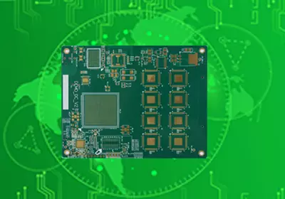
Repairing PCB boards is often possible when the damage is limited to a broken trace, defective solder joint, damaged pad, or failed component. However, a successful repair depends on identifying the actual cause of the failure before any rework begins. A circuit board that appears to have a simple broken connection may also have damaged vias, internal layer connections, or laminate beneath the visible surface. For this reason, PCB repair should begin with inspection and electrical testing rather than immediately applying heat or solder.
The repair method also depends on the construction and electrical function of the board. A simple single-layer board can usually be approached differently from a multilayer PCB with fine-pitch components, controlled-impedance traces, buried vias, or high-density interconnects. The objective is not simply to make two points electrically conductive again, but to restore the circuit without creating new mechanical, electrical, or reliability problems.
Identifying the Cause of PCB Board Damage
Before repairing a PCB board, it is necessary to determine what caused the failure. Physical damage is relatively easy to recognize when a copper trace has been visibly broken or a component has been burned, but many PCB failures are not obvious from visual inspection alone. A board that does not power up, resets unexpectedly, or produces an intermittent signal may have an electrical fault that cannot be identified by looking at the surface.
A careful inspection should therefore examine the board for cracked traces, lifted pads, damaged vias, solder bridges, poor solder joints, burned laminate, corrosion, missing components, and signs of previous rework. Magnification can be useful when working with fine-pitch components because small cracks and solder defects can be difficult to see without it.
Electrical measurements should then be used to confirm the suspected fault. A multimeter can determine whether a trace or connection is continuous and can help identify an unexpected short circuit. When a power-related failure is suspected, checking the input voltage and following the relevant power rails can narrow down the location of the problem. More complex boards may require an oscilloscope or other test equipment to examine clocks, communication signals, switching waveforms, and other circuit functions.
This diagnostic stage is particularly important because repairing the wrong area can introduce additional damage. Applying excessive heat to a healthy pad or removing a component unnecessarily can weaken the PCB and make the original problem more difficult to resolve.
Repairing a Broken PCB Board Trace
A broken copper trace is one of the more straightforward PCB board faults to repair when the surrounding laminate remains in good condition. The first step is to identify both sides of the damaged section and confirm that the two points are supposed to be electrically connected.
A small area of solder mask can then be removed from the copper on both sides of the break. The exposed copper should be clean and free from oxidation before a suitable flux is applied. Depending on the width and electrical function of the original trace, a short section of wire may be used to bridge the damaged area. The repair wire should be positioned so that it does not place unnecessary mechanical stress on the original copper.
After soldering, continuity should be checked again. However, continuity alone does not prove that the repair has restored the original electrical characteristics. This distinction becomes important when repairing high-speed digital, RF, or other controlled-impedance circuits. A jumper wire may reconnect a broken circuit while simultaneously changing its impedance, parasitic capacitance, inductance, or signal path. In such applications, the repair must be evaluated according to the function of the original routing rather than continuity alone.
Repairing a Damaged PCB Pad
A damaged PCB pad requires more attention because the pad provides both an electrical connection and a mechanical attachment point for the component. Pads can lift from the laminate when excessive heat or mechanical force is applied during soldering and desoldering. Once a pad has separated from the board surface, simply adding more solder will not restore the original structure.
The repair approach depends on how much of the original copper remains attached to the board. If part of the pad and its connection are still intact, the damaged area may be stabilized and electrically reinforced. When the entire pad has been removed, the connection may need to be reconstructed using an appropriate conductive repair method and secured against mechanical movement.
The condition of the laminate around the damaged pad should also be examined. If the substrate has been burned, cracked, or delaminated, the visible pad may not be the only problem. In that situation, replacing the connection without addressing the substrate damage can result in an unreliable repair.
Repeated component removal is another common cause of pad failure. When a component must be removed from a PCB board, controlling the temperature and minimizing mechanical force can significantly reduce the risk of lifting pads or damaging the surrounding solder mask.
Repairing PCB Board Solder Joints
Some PCB board failures originate from solder joints rather than the board material itself. A cracked solder joint can produce intermittent electrical contact, particularly when the assembly is exposed to vibration, thermal cycling, or mechanical stress. Poor wetting, insufficient solder, solder bridging, and excessive solder can also cause electrical or mechanical problems.
A defective solder joint should first be inspected to determine whether the component and pad are still mechanically sound. If the connection is otherwise intact, controlled reflow or rework may restore the joint. The repaired connection should then be tested under the conditions that originally produced the failure.
Fine-pitch packages require greater care because the solder connections may be difficult to inspect directly. Components such as QFNs and BGAs can require controlled heating and specialized rework equipment, particularly when the board contains a large number of closely spaced connections. Repeated heating cycles can also affect the PCB laminate and nearby components, so unnecessary rework should be avoided.

Repairing a Damaged PCB Via
A via provides an electrical connection between different conductive layers of a PCB board. When a via is damaged, the problem may not be visible from the surface because part of the electrical connection can exist inside the board.
A continuity test can help determine whether the expected connection between layers is still present. If the via has failed, the appropriate repair depends on its construction, location, current requirements, and accessibility. A through-hole via is generally easier to diagnose and repair than a blind or buried via because the complete electrical path is not readily accessible from the surface.
This becomes particularly important in multilayer PCB repair. The external appearance of the board may remain relatively normal even when an internal layer connection has been damaged. In such cases, the original schematic, PCB layout, stack-up information, and fabrication data can provide valuable information about the intended electrical path.
Repairing Burned or Corroded PCB Board Areas
Burn marks on a PCB board usually indicate that the board has experienced excessive current, excessive temperature, component failure, or another abnormal operating condition. Repairing the visible damage without identifying the original cause can result in another failure after the board is returned to service.
The damaged area should be inspected to determine whether the copper, solder mask, and laminate have been affected. Minor surface contamination or corrosion may be removable when the underlying materials remain intact. More severe thermal damage is more difficult because the laminate itself may have lost its mechanical and electrical properties.
Corrosion also requires attention to the source of contamination. Moisture, chemicals, flux residues, and environmental exposure can all contribute to corrosion. If the cause is not removed, a repaired connection may deteriorate again even when the immediate electrical fault has been corrected.
When PCB Repair Is Not the Best Option
Not every damaged PCB should be repaired. A repair can become impractical when several internal layers are damaged, the laminate has suffered severe thermal degradation, or the board contains critical structures whose original electrical characteristics cannot be reproduced reliably.
High-speed and RF boards require particular caution because changes to trace geometry, dielectric structure, grounding, or via configuration can affect signal integrity. A repair that restores DC continuity may still cause excessive insertion loss, impedance discontinuity, crosstalk, or other performance problems.
The same consideration applies to high-reliability applications. When a PCB is used in an environment where failure could have significant operational consequences, the decision to repair should consider the expected reliability of the repaired structure rather than only the immediate repair cost.
In some cases, manufacturing a replacement PCB is more practical than attempting to restore a severely damaged board. If the original design files and fabrication information are available, reproducing the board can provide a more predictable result than performing extensive component-level repairs.
How to Verify a PCB Repair
A PCB board should not be considered successfully repaired simply because the damaged area looks correct. Electrical and functional testing should confirm that the repaired circuit behaves as intended.
Continuity measurements can verify basic electrical connections, while resistance measurements can help identify unexpected shorts or abnormal paths. Power rails should be checked before connecting sensitive components or applying full operating voltage. If the board contains high-speed interfaces, analog circuitry, switching power supplies, or other sensitive functions, additional functional testing may be necessary.
The repaired area should also be inspected for mechanical stability. A wire bridge that moves when the board is handled may eventually fail even though it initially passes an electrical test. The repair should therefore be secured appropriately and positioned so that vibration, thermal expansion, and normal handling do not place excessive stress on the repaired connection.
For boards used in production equipment, documenting the failure and repair can also be valuable. Recording the original fault, the repair method, test results, and final operating condition makes future troubleshooting more efficient and helps determine whether the same failure is likely to occur again.
Preventing PCB Board Damage During Rework
Many PCB board failures occur during repair rather than during normal operation. Excessive soldering temperature, prolonged heating, aggressive component removal, and excessive mechanical force can damage copper pads and laminate materials.
Controlled thermal management is therefore important whenever components are removed or replaced. The objective is to transfer enough heat to achieve the required soldering or desoldering process without unnecessarily heating the surrounding PCB. Appropriate tools and techniques should be selected according to the component package, board thickness, copper distribution, and thermal characteristics of the assembly.
Mechanical handling is equally important. Flexible areas should not be bent unnecessarily, and repaired traces or wires should be supported when movement could place stress on the solder joint. Keeping the repair area clean also helps prevent contamination from affecting solderability or electrical insulation.
Repair or Replace the PCB Board?
The decision to repair or replace a PCB board should ultimately be based on the extent of damage, the complexity of the circuit, the required reliability, and the availability of replacement boards or manufacturing data. A broken trace or isolated solder defect may be worth repairing, especially when the board is otherwise in good condition. A severely burned multilayer board with multiple damaged interconnections may require considerably more engineering effort than the value of the repair justifies.
For obsolete equipment, however, PCB repair or reproduction can be useful when replacement boards are no longer available. In these situations, understanding the original circuit architecture and manufacturing structure becomes more important than simply restoring a visible connection.
The most reliable approach is to diagnose the failure first, select a repair method that matches the electrical and mechanical requirements of the pcb board, and verify the result through appropriate testing. Repairing PCB boards is not simply a matter of reconnecting damaged copper; the repair must restore the function and reliability of the circuit without creating a new failure elsewhere on the board.