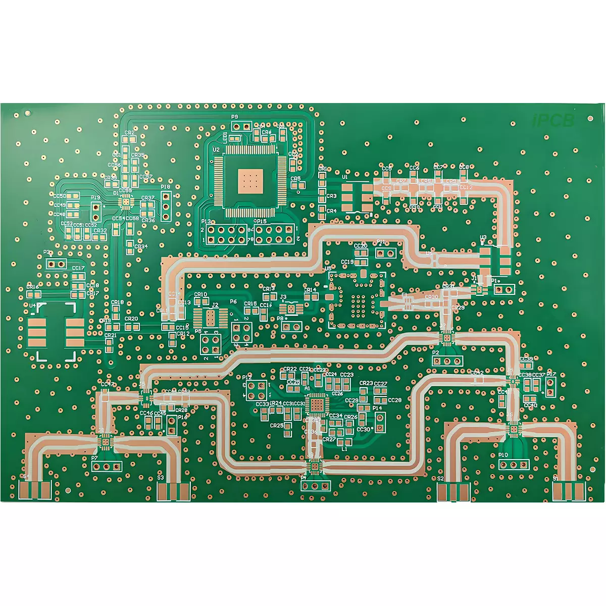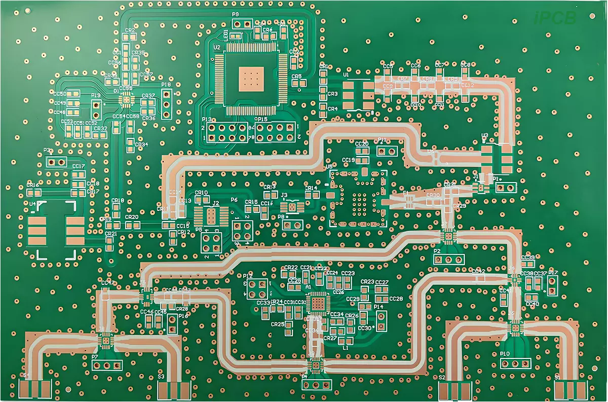
Product Name: Induction PCB
Material:RF PCB material
Quality standard: IPC 6012
PCB material Dk: 2.2-16
Thickness: 0.1mm - 1.6mm
Copper thickness: 0.5oz - 1oz
Surface technology: Silver, Gold, OSP
Layer: 1Layer PCB, 2Layers PCB, multilayer PCB
Material composition: Ceramic, Teflon, FR-4
Application: RF microwave PCB
Induction PCB is an indispensable component of modern electronic devices, and its quality and performance directly affect the stability and reliability of the equipment. We will elaborate on the production techniques of Induction PCB from four aspects, including circuit design, component selection, layout optimization, and soldering technology. By learning these techniques, readers will be able to master important skills and practical experience in producing high-quality Induction PCB.
1. Circuit Design
Circuit design is the foundation of Induction PCB production, which is related to the functionality and performance of the circuit. Accurate power consumption estimation is required to determine the appropriate power supply voltage and power consumption control method based on the characteristics of the sensor. In circuit design, signal strength and impedance matching issues should be considered, and filtering circuits and amplifier circuits should be selected reasonably to ensure accurate signal acquisition and transmission. Attention should also be paid to the stability and anti-interference ability of the circuit, and the power filtering circuit and anti-interference components should be reasonably set to reduce the sensitivity of the circuit to external interference.
2. Component selection
The selection of components has a significant impact on the performance and reliability of the Induction PCB. According to the requirements of the sensor circuit, suitable sensors and chips should be selected to ensure their appropriate accuracy and stability. It is also necessary to choose suitable components such as resistors, capacitors, inductors, etc. to meet the functional requirements of the circuit. When selecting components, it is also necessary to consider the quality and availability of the components, and choose suppliers and brands with good reputation to ensure the reliability of the components.
3. Layout optimization
The layout of the circuit board is equally crucial for the performance and reliability of the Induction PCB. To plan the layout of the circuit board reasonably, separate the power, ground, and signal lines to reduce the probability of mutual interference. Also, it is important to isolate sensitive signal lines from noise sources to reduce the possibility of signal crosstalk. In the layout process, it is also important to pay attention to the position of components and the length of wiring, try to shorten the length of signal lines and reduce the number of layers on the circuit board to reduce signal attenuation and impedance matching issues.
4. Welding technology
Welding is an essential step in the production of Induction PCB, directly affecting the quality and reliability of circuit connections. To ensure welding quality and reliability, it is necessary to choose appropriate welding processes and equipment, and master the correct welding temperature and time. Attention should be paid to the welding process requirements, including the layout of welding points, alignment of components, and cleaning of welding surfaces. During the welding process, attention should also be paid to preventing overheating and over welding to avoid damaging components and circuit boards. Attention should also be paid to checking the quality of welding points and promptly repairing and handling welding defects.

Induction PCB
Circuit design, component selection, layout optimization, and soldering techniques are key elements in producing high-quality Induction PCB.
Product Name: Induction PCB
Material:RF PCB material
Quality standard: IPC 6012
PCB material Dk: 2.2-16
Thickness: 0.1mm - 1.6mm
Copper thickness: 0.5oz - 1oz
Surface technology: Silver, Gold, OSP
Layer: 1Layer PCB, 2Layers PCB, multilayer PCB
Material composition: Ceramic, Teflon, FR-4
Application: RF microwave PCB
iPCB Corporation provides support for PCB Prototype and Electronic Manufacturing. You can request consultation or quotation for PCB, PCBA and ODM here, please contact email: sales@ipcb.com
We will respond very quickly.