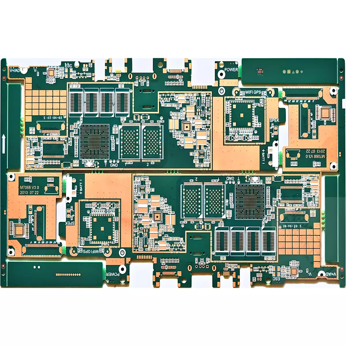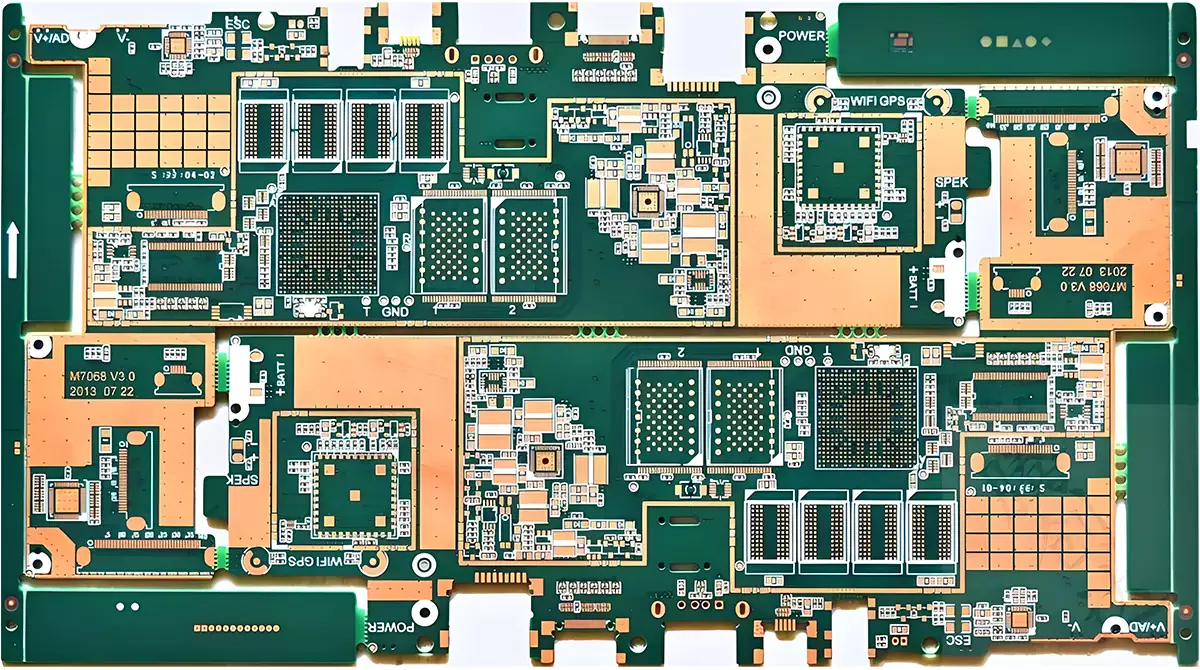
Product Name:Mobile PCB
Material:FR-4,PTFE
Thickness: 1.2mm
Copper thickness: 0.5OZ
Surface technology: Enig/OSP
Solder mask: White/Blue
Silk screen: White
Minimum line width/spacing: 3mil
Minimum through-hole: 25um
Application: Mobile PCB
A mobile pcb is a critical component used to link and assemble the internal circuits of a mobile phone.It is generally a thin,insulated substrate with a conductive layer on the surface, which is used to connect and support a variety of electronic devices inside a mobile phone, such as the processor, storage, sensors and antennas. The core functions of a mobile pcb board include establishing electrical connections, providing mechanical support, implementing thermal management,and ensuring effective communication and data transfer between electronic devices.
The core materials for mobile pcb includes FR-4 glass fibre boards and high-frequency boards, which are widely used in most conventional mobile phones due to their outstanding thermal stability, excellent mechanical strength and good electrical properties. For mobile phones that need to transmit high-frequency signals, such as 5G mobile phones, high-frequency boards made of PTFE are preferred, which have extremely low dielectric loss and excellent high-frequency response.
Generally, PCBs (Printed Circuit Boards) in mobile phones are designed with a four- or six-layer structure. The design of a four-layer PCB is relatively simple and consists of two layers: the top layer usually contains the main chips, signal lines and components such as the keypad, while the bottom layer is mainly responsible for connecting the battery, power supply and other modules. Early mobile phones used a four-layer PCB design, but now it has almost been replaced by a six-layer PCB.
The structure of the six-layer PCB is more complex, in addition to the top and bottom layers,but also contains four additional layers of internal wiring layer, these internal layers are mainly used for connecting the chip, signal transmission and connecting the display and other modules.The top and bottom layers are mainly used for arranging signal connection, power supply and important modules, as well as digital camera, accessory interfaces, etc., while the four internal layers are mainly used for arranging processors,memory,wireless communication modules and other electronic components.
In the process of mobile pcb design, designers will be based on the layout of the various levels to develop specific wiring and transfer strategy to ensure that the communication effect between the modules and the ability to send and receive external signals more excellent.
In general,the layout of mobile phone pcb has an important impact on the signal transmission, operational efficiency and power consumption of mobile phones. With the continuous progress of mobile phone technology,pcb board structure and layout mode is also in the continuous optimisation and improvement.

Working principle:
Circuit board is the central nervous system of the whole mobile phone,bears the important task of shunting, distributing and transmitting signals.CPU,as the core computing and processing part of the whole system,works in concert with other components,together with the different operating systems carried by different chips,can quickly process high-speed information such as images,sound, etc.,and according to the instructions to complete the corresponding functions,so as to let the mobile phone to achieve a variety of rich and colourful applications.
Features and functions:
1.Multi-layer structure:in order to meet the wiring requirements of the complex circuits inside the mobile phone, mobile phone pcb board usually uses a multi-layer structure, with two, four or more layers. Multi-layer structure can provide greater wiring density, reduce the size of the pcb board, and improve the performance and stability of the circuit.
2.High-density wiring: with the increasing functionality and decreasing size of mobile phones,mobile pcb needs to achieve a higher density of wiring to ensure that the connection and communication between the various functional modules. High-density wiring requires pcb board manufacturing process and materials with high precision and high reliability.
3.High-speed signal transmission:mobile pcb board needs to support high-speed signal transmission to meet the requirements of high-speed processors, memory and communication modules. In order to ensure stable transmission of high-speed signals and low signal attenuation, mobile phone pcb usually uses special materials and processes, such as low dielectric constant materials, microstrip line design.
4.Special function design: in addition to connecting and supporting various electronic components,mobile phone pcb board may also integrate some special function design, such as antenna design, power management, signal filtering, protection circuit and so on.These designs can improve the performance, stability and user experience of mobile phones.
5.Small size and lightweight:Since the mobile phone pcb board needs to be installed inside the mobile phone, it needs to have a small size and lightweight features to adapt to the mobile phone's compact design and thin and light appearance requirements.
Market Trends
With the booming expansion of the mobile phone market, the demand for mobile PCB continues to climb, and the market demand shows a strong trend. It is predicted that the mobile phone PCB board market will maintain a high growth rate in the coming years. However, the price of mobile phone PCB boards is expected to level off due to the dual impact of technological innovation and market competition. At the same time, in the face of growing market demand, suppliers are actively taking measures to reduce production costs and improve production efficiency, in order to take advantage of the fierce competition in the market.
Product Name:Mobile PCB
Material:FR-4,PTFE
Thickness: 1.2mm
Copper thickness: 0.5OZ
Surface technology: Enig/OSP
Solder mask: White/Blue
Silk screen: White
Minimum line width/spacing: 3mil
Minimum through-hole: 25um
Application: Mobile PCB
iPCB Corporation provides support for PCB Prototype and Electronic Manufacturing. You can request consultation or quotation for PCB, PCBA and ODM here, please contact email: sales@ipcb.com
We will respond very quickly.