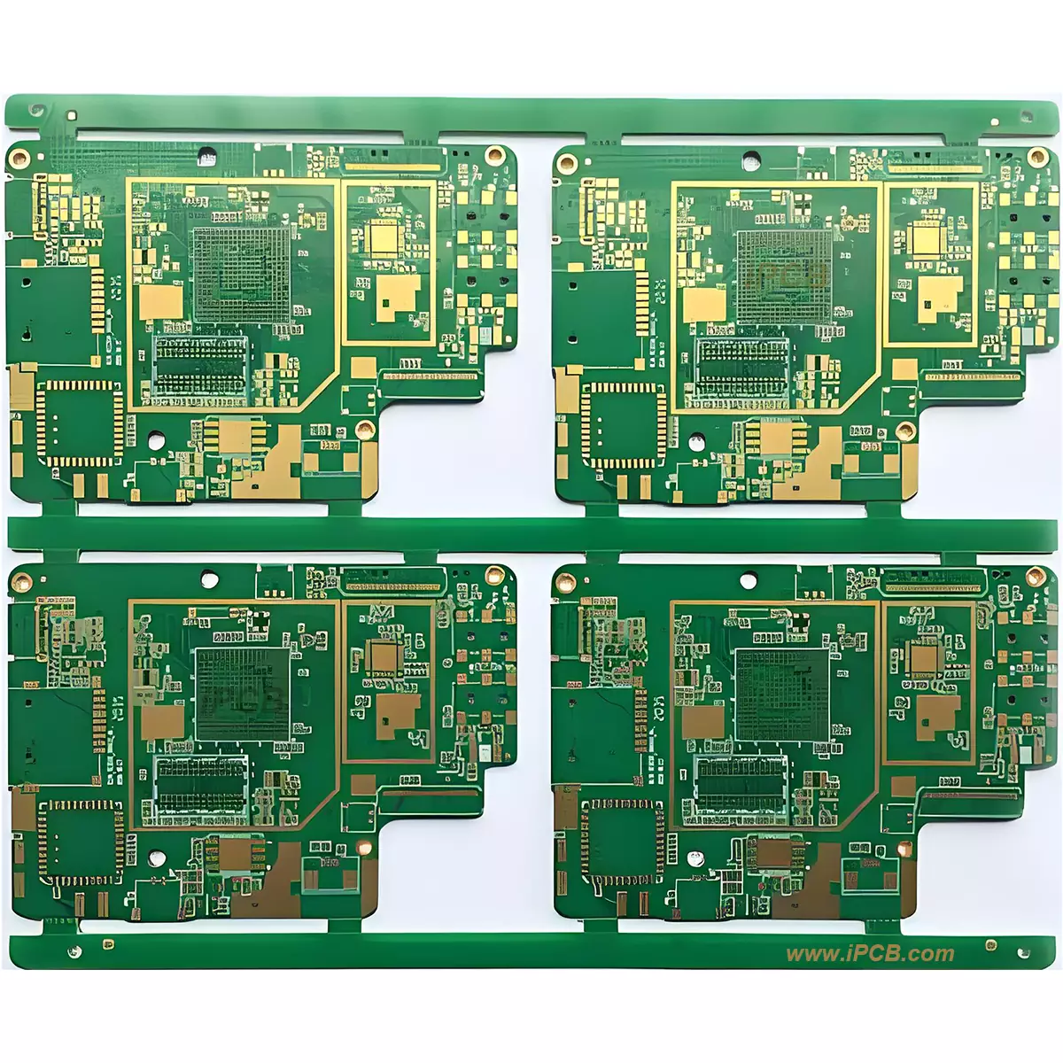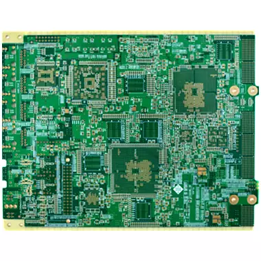

Product Name: Multilayer PCB
Material: S1000-2 or IT180
Layers: 4-12L
Thickness: 1.0mm
Copper thickness: 1/H/H/1oz
Surface technology: Glod
Solder mask: Green
Silk screen: White
Minimum line width/spacing: 3/3mil
Minimum through-hole: 0.2mm
Application: Android digital products
What is multilayer PCB?
Multilayer PCB refers to a PCB circuit board with two or more layers. It is composed of connecting wires on several insulated PCB and solder pads used for assembling and soldering electronic components. It not only conducts the circuits of each layer, but also has the function of mutual insulation.
Multilayer PCB board has multiple wiring layers, with a dielectric layer between every two layers, which can be made very thin. A multilayer circuit board has at least three conductive layers, with two layers on the outer surface and the remaining layer synthesized inside the insulation board. The electrical connection between them is usually achieved through plated through holes on the cross-section of the circuit board.
The process difficulty and processing price of circuit board are determined by the number of wiring surfaces. Ordinary circuit board are divided into single-sided wiring and double-sided wiring, commonly known as single panel and double-sided board. However, high-end electronic products are limited by product space design factors. In addition to surface wiring, multiple layers of circuits can be stacked inside. During the production process, after each layer of circuit is made, it is then positioned and pressed by optical equipment to stack multiple layers of circuits on one circuit board. Commonly known as multilayer circuit board. Any circuit board with more than or equal to 2 layers can be called a multilayer PCB. Multilayer PCB circuit board can be divided into multilayer rigid circuit board, multilayer soft hard circuit board, and multilayer soft hard combination circuit board.
Due to the increase in packaging density of integrated circuits, the high concentration of interconnects has made the use of multilayer PCB necessary. Unforeseeable design issues such as noise, stray capacitance, crosstalk, etc. have occurred in the layout of printed circuits. Therefore, the design of printed circuit board must strive to minimize the length of signal lines and avoid parallel routes. Obviously, in single panel or even double-sided PCB, due to the limited number of intersections that can be achieved, these requirements cannot be satisfactorily answered. In the case of a large number of interconnections and cross requirements, in order for a circuit board to achieve satisfactory performance, it is necessary to expand the board layers to two or more layers, resulting in the emergence of multilayer circuit board. Therefore, the original intention of manufacturing multilayer circuit board is to provide more degrees of freedom in selecting appropriate distribution paths for complex and/or noise sensitive electronic circuits. A multilayer circuit board has at least three conductive layers, with two layers on the outer surface and the remaining layer synthesized inside the insulation board. The electrical connection between them is usually achieved through plated through holes on the cross-section of the circuit board. Unless otherwise specified, multilayer printed circuit board, like double-sided board, are generally plated with through-hole board.
Multilayer PCB is manufactured by stacking two or more circuits on top of each other, with reliable pre-set interconnections between them. Due to the completion of drilling and electroplating before all layers are compacted together, this technology violates the traditional manufacturing process from the beginning. The innermost two layers are composed of traditional double-sided PCB, while the outer layers are different as they are composed of independent single PCB. Before compaction, the inner PCB will be drilled, plated through holes, pattern transferred, developed, and etched. The outer layer of the drilled hole is the signal layer, which is plated through by forming a balanced copper ring on the inner edge of the through-hole. Subsequently, each layer is rolled together to form a multilayer circuit board, which can be connected to each other (between components) using wave soldering.
The use of multilayer PCB board is in professional electronic equipment (computers, military equipment), especially in situations where the weight and volume are overloaded. However, this can only be achieved by increasing the cost of multilayer PCB board in exchange for an increase in space and a reduction in weight. In high-speed circuits, multilayer PCB is also very useful, as they can provide printed circuit board designers with more than two layers of board surface to lay wires and provide large grounding and power areas.
The trend of multilayer PCB board development
1. High density
2. Thin and multilayered design
3. Diversification of multilayer PCB structures
4. Thin substrate for high-performance thin copper boxes
5. High flatness of board surface and surface coating technology
6. Flexible multilayer PCB board and rigid flexible multilayer PCB board
Characteristics of multilayer PCB
The biggest difference between multilayer PCB board and single layer PCB or double sided PCB is the addition of an internal power layer (to maintain the internal electrical layer) and a ground layer. The power and ground networks are mainly wired on the power layer. However, the wiring of multilayer PCB board is mainly based on the top and bottom layers, supplemented by the middle wiring layer. Therefore, the design method of multilayer PCB board is basically the same as that of double sided PCB board, and the key is how to optimize the wiring of the inner layer, making the wiring of the circuit board more reasonable and the electromagnetic compatibility better.
Quality assurance of multilayer PCB
The quality of multilayer circuit board is defined in IPC, and the surface process is anti-oxidation. If the vacuum packaging is not removed, it should be used up within six months. If the vacuum packaging is removed, it should be used up within 24 hours, and in an environment with controlled temperature and humidity, the board should be used up within one year. If the packaging is removed, the board should be pasted up within one week. Temperature and humidity should also be controlled. Gold PCB board are equivalent to tin board, but the control process is stricter than tin PCB board.
How to choose a multilayer PCB manufacturer?
The processing of multilayer circuit board is generally outsourced, so when providing drawings for outsourced multilayer PCB processing, it is necessary to be accurate and as clear as possible. Attention should be paid to material selection, lamination sequence, board thickness, tolerance requirements, processing technology, and so on. When exporting GERBER from multilayer PCB, it is recommended to use RS274X format for exporting data.
Product Name: Multilayer PCB
Material: S1000-2 or IT180
Layers: 4-12L
Thickness: 1.0mm
Copper thickness: 1/H/H/1oz
Surface technology: Glod
Solder mask: Green
Silk screen: White
Minimum line width/spacing: 3/3mil
Minimum through-hole: 0.2mm
Application: Android digital products
iPCB Corporation provides support for PCB Prototype and Electronic Manufacturing. You can request consultation or quotation for PCB, PCBA and ODM here, please contact email: sales@ipcb.com
We will respond very quickly.