Share cost-effective products and high-quality services with customers. Contact Us


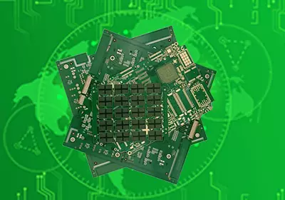
A multilayer PCB for communication applications provides additional copper layers for signal routing, power distribution, and reference planes, allowing engineers to build more controlled electrical paths within a limited board area. The value of the multilayer structure is therefore not simply the number of layers. It is the ability to manage routing density, signal integrity, power integrity, electromagnetic compatibility, and mechanical constraints as part of the same PCB structure.
Why Communication Equipment Uses Multilayer PCBs
A communication PCB often needs to accommodate processors, memory, transceivers, connectors, power circuits, clock networks, and high-speed interfaces on a relatively compact board. Trying to route all of these connections on only one or two copper layers can create long signal paths, crowded routing areas, insufficient reference planes, and greater opportunities for unwanted coupling between circuits. Additional layers allow different signal groups and power networks to be distributed through the board while keeping important signal paths closer to their reference planes.
This layer structure becomes particularly important when the board carries high-speed digital signals. A fast signal should not be viewed simply as electrical current traveling through a copper trace. Once the signal edge becomes sufficiently fast, the trace behaves as part of a transmission line, and the geometry of the trace and its surrounding dielectric structure directly affects impedance and signal propagation. IPC guidance for controlled-impedance PCB design identifies parameters such as conductor width and thickness, dielectric thickness, and dielectric constant as factors that determine characteristic impedance.
A multilayer communication PCB can therefore place signal layers next to continuous reference planes and use dedicated power or ground structures to create more predictable electrical environments. This also helps establish shorter return-current paths. A well-planned stack-up can reduce unnecessary loop area and help limit coupling between neighboring circuits, although the final performance still depends on routing geometry, layer transitions, material properties, and the complete system design. Current multilayer PCB design guidance likewise treats stack-up planning as a foundation for impedance control, signal integrity, and EMI performance.
Stack-Up and Signal Integrity in Communication PCBs
The stack-up is one of the earliest decisions in a multilayer PCB design because it determines the physical relationship between signal traces, reference planes, dielectric materials, and power distribution. For communication equipment, the layer arrangement needs to be developed around the actual interfaces and their electrical requirements rather than simply selecting a layer count and beginning the routing process.
High-speed differential pairs are a common example. When a communication link depends on controlled differential signaling, the two conductors need consistent geometry and an appropriate reference structure throughout the route. Changes in trace width, spacing, dielectric thickness, layer transition, or reference-plane continuity can introduce impedance discontinuities. Vias can also affect high-speed signals because a transition between layers changes the electromagnetic environment of the transmission line. At sufficiently high bandwidths, via transitions and unused via sections can contribute to reflection and loss and therefore need to be considered during layout.
The choice of PCB material is closely connected to this issue. A communication board operating at moderate speeds may be adequately served by a conventional material system, while higher-frequency or higher-data-rate designs may require tighter control of dielectric properties and transmission loss. The appropriate material should be selected according to operating frequency, signal rise time, required impedance, insertion-loss budget, thermal conditions, and manufacturing capability rather than simply choosing the material with the lowest dielectric constant.
Ground and power structures also deserve careful attention. A continuous reference plane gives high-speed signals a defined return path, while interruptions in that reference structure can force return currents to take longer paths and increase coupling or electromagnetic radiation. This is why multilayer communication PCB design generally treats signal routing, reference planes, and power distribution as one interconnected problem rather than separate layout tasks.

Design Requirements for Different Communication Circuits
The exact PCB structure depends heavily on the type of communication system. A board used for conventional wired communication may prioritize high-density connectors, Ethernet or other high-speed interfaces, power distribution, and controlled impedance. A wireless communication board may place greater emphasis on RF transmission lines, antenna interfaces, isolation between noisy digital circuits and sensitive RF sections, and stable dielectric characteristics. More complex equipment can combine these requirements on the same multilayer board.
For high-speed digital communication, the designer needs to consider the complete signal path from transmitter to receiver. Trace length, impedance, differential-pair geometry, layer transitions, vias, connectors, and reference-plane continuity can all contribute to the final signal quality. As data rates increase, insertion loss, return loss, crosstalk, and timing margins become increasingly important. Recent high-speed PCB design references also emphasize that the electrical behavior of a multilayer board is strongly influenced by stack-up, impedance control, differential routing, and loss management.
RF communication introduces another set of requirements. RF traces need a controlled electromagnetic environment, and their relationship with the surrounding ground structure and dielectric material can influence impedance and loss. When RF circuits share a board with digital processors, switching power supplies, clocks, and other noise sources, physical separation and appropriate reference structures can help reduce unwanted coupling. The multilayer structure can provide dedicated regions and planes for these functions, but it does not automatically solve EMI or RF isolation problems. Component placement, routing, grounding, shielding, and filtering still have to be considered together.
Communication equipment can also require HDI structures when component density becomes too high for conventional through-hole interconnections. Microvias and finer interconnection structures can shorten connections and provide additional routing flexibility, particularly around fine-pitch packages. Whether HDI is necessary depends on component density, board size, layer count, signal requirements, and manufacturing capability. The underlying principle remains the same: the interconnection structure should support the electrical performance required by the communication system without creating manufacturing conditions that are difficult to control.
Manufacturing a Multilayer PCB for Communication Equipment
The manufacturing process needs to preserve the electrical characteristics established during the design stage. A multilayer communication PCB is built by combining copper layers, dielectric materials, and conductive interconnections into a controlled stack-up. Layer alignment, dielectric thickness, copper thickness, via formation, plating, and surface finishing all influence the final structure. Small manufacturing variations can become more significant when the board contains tightly controlled impedance structures or high-speed transmission paths.
Impedance control is therefore not only a layout requirement. The fabricated board has to reproduce the geometry defined in the stack-up. Trace width, copper thickness, dielectric thickness, and material properties all contribute to the resulting impedance. For production designs, communication PCB specifications may therefore include controlled-impedance requirements and appropriate verification methods rather than relying solely on nominal CAD dimensions.
Manufacturability should also be considered before routing is finalized. A stack-up with extremely thin dielectric layers, fine traces, small vias, high layer counts, or demanding impedance tolerances may require tighter process control. The design should account for the capabilities of the selected fabrication process, including registration, drilling, plating, lamination, copper distribution, and testing. Symmetrical layer structures and balanced copper distribution can also help manage mechanical behavior during fabrication and thermal processing.
A well-designed multilayer PCB for communication is therefore the result of coordination between circuit requirements and physical board construction. The number of layers should provide enough routing capacity without adding unnecessary complexity, while the stack-up should establish appropriate reference planes, impedance structures, and power-distribution paths. Material selection, via design, differential routing, RF isolation, and manufacturing tolerances then need to be considered within the same framework.
For communication equipment, the PCB is part of the signal-transmission system rather than simply a platform that connects components. A properly engineered multilayer structure can provide the routing density needed for complex hardware while giving designers greater control over signal integrity, power distribution, EMI behavior, and high-speed interconnections. The most suitable construction ultimately depends on the communication interface, operating frequency, data rate, component density, thermal requirements, board dimensions, and manufacturing constraints of the specific design.