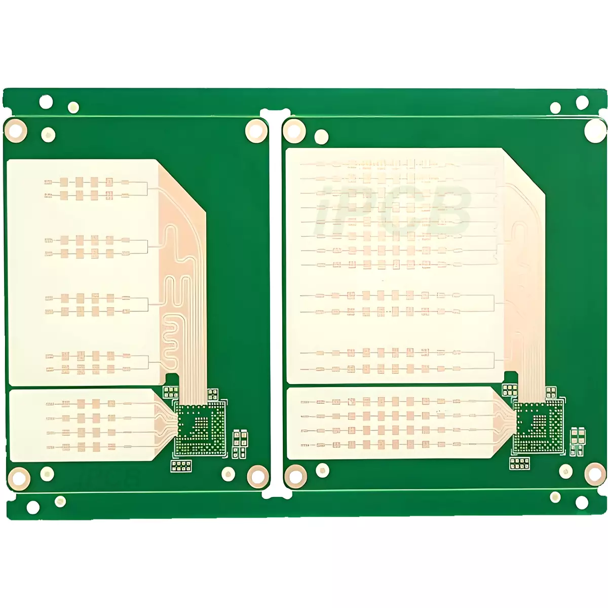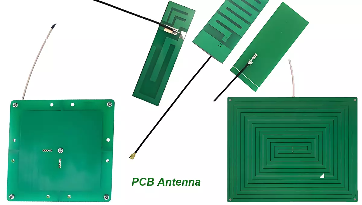
Product Name: PCB Antenna
Material: Ceramic, Teflon, FR-4
Quality standard: IPC 6012
Rogers PCB material Dk: 2.2-16
Layer: 1L, 2layer PCB, multilayer PCB
Thickness: 0.1mm - 12mm
Copper thickness: 1oz
Surface technology: Silver, Gold,
Application: RF, microwave, radar
There are many types of antenna to choose from in an RF product. When choosing an antenna, size, cost, and performance are the most important factors. The three common short-range antenna devices are PCB antenna, chip antenna, and whip antenna with a connector.
Characteristics of Three Common antenna
1. PCB antenna
Considering cost factors, the most suitable option is PCB antenna. Designing a PCB antenna is usually not easy and requires the use of simulation tools to achieve an acceptable solution. In order to obtain the best design, it is difficult and time-consuming to configure the simulation tool to the accurate simulation state. Therefore, when the space of the PCB antenna board is sufficient, you can refer to the existing scheme. There are many 2.4GHz antenna design schemes available on the Internet for reference.
2. Chip antenna
If the size of the PCB board has limitations on the antenna, a chip antenna can be chosen. This total antenna allows for wireless frequencies of 1GHz to be achieved in small-sized solutions. Compared to PCB antenna, this type of antenna increases BOM and monitoring costs. Even though the manufacturer of the chip antenna claims that the chip antenna matches a characteristic resistance of 50 Ω in the characteristic frequency band, additional matching circuits are still needed in practical applications to achieve appropriate performance.
3. Whip antenna
If performance is the primary consideration and compromises can be made in terms of size and cost, then an external connector connected antenna is a good solution. This type of antenna is usually monopole and has an omnidirectional radiation pattern. That is to say, this type of antenna has similar performance in all directions. The price of whip antenna is significantly higher than that of chip antenna, and an additional connector needs to be added on the PCB board, which also increases the cost.

What is PCB antenna?
PCB antenna, also known as printed circuit board antenna, is a type of antenna that is directly printed on a PCB (printed circuit board). This type of antenna plays an increasingly important role in modern wireless communication devices, especially in mobile devices, IoT devices, and wireless sensor networks. Due to its compact, lightweight, and low-cost characteristics, it has been widely used.
The design principle of PCB antenna is based on electromagnetic field theory. By arranging specific metal conductor patterns on the PCB board, effective electromagnetic radiation and reception structures can be formed, thereby achieving wireless signal transmission and reception. The performance of PCB antenna is influenced by various factors, including the shape, size, material of the conductor pattern, and the dielectric properties of the PCB board. Therefore, when designing PCB antenna, it is necessary to comprehensively consider these factors to ensure that the antenna's performance meets practical application requirements.
There are various types of PCB antenna, including dipole antenna, monopole antenna, loop antenna, slot antenna, etc. These antenna forms each have their own advantages and disadvantages, and are suitable for different application scenarios. For example, dipole antenna have good radiation performance and stability, making them suitable for general wireless communication devices; The monopole antenna, on the other hand, has a smaller size and lower cost, making it suitable for miniaturized and low-cost application scenarios. In practical applications, the design and optimization of PCB antenna is a critical task. Designers need to select appropriate antenna forms and parameters based on specific wireless communication standards, device dimensions, performance requirements, and other factors, and conduct detailed simulations and tests. By continuously optimizing antenna design, the performance, stability, and reliability of wireless communication devices can be improved.
In practical applications, PCB antenna also need to be coordinated with other wireless communication device components, such as RF transceivers, filters, power amplifiers, etc. Therefore, for the design and application of PCB antenna, comprehensive wireless communication knowledge and technical background are required. At the same time, it is also necessary to pay attention to the development trends and market demands of wireless communication technology, constantly innovate, and contribute to the development of the wireless communication field. The production and installation of PCB antenna is also an important task. During the production process, it is necessary to ensure the quality of the PCB board, the accuracy and consistency of the conductor pattern, and other factors to ensure the performance of the antenna. When installing, it is necessary to consider the position, direction, impedance matching, and other issues of the antenna to ensure that it can be effectively integrated with other parts of the wireless communication device.
The new wireless communication standards and technologies have put forward higher requirements for the performance of PCB antenna. With the continuous progress of PCB board manufacturing technology and the continuous reduction of costs, PCB antenna will also be applied in more fields.
Product Name: PCB Antenna
Material: Ceramic, Teflon, FR-4
Quality standard: IPC 6012
Rogers PCB material Dk: 2.2-16
Layer: 1L, 2layer PCB, multilayer PCB
Thickness: 0.1mm - 12mm
Copper thickness: 1oz
Surface technology: Silver, Gold,
Application: RF, microwave, radar
iPCB Corporation provides support for PCB Prototype and Electronic Manufacturing. You can request consultation or quotation for PCB, PCBA and ODM here, please contact email: sales@ipcb.com
We will respond very quickly.