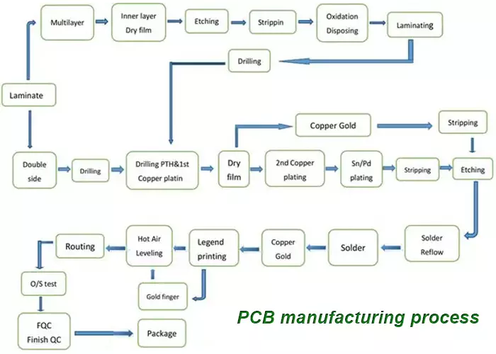
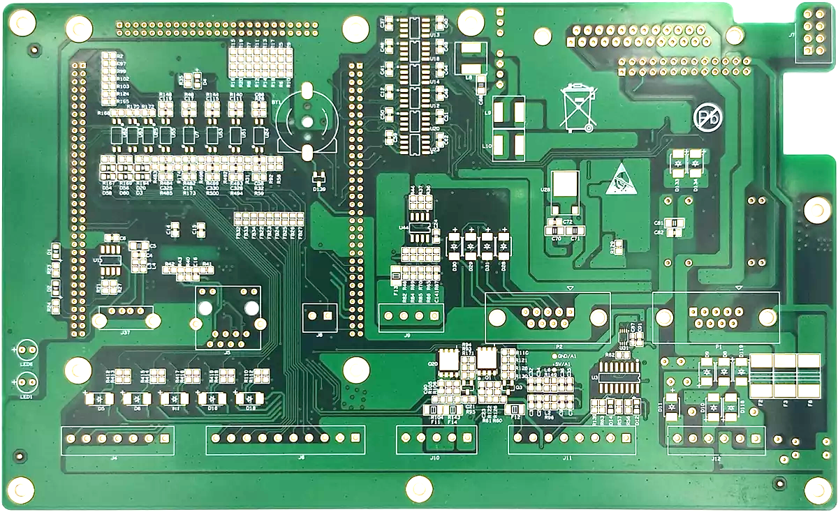
PCB manufacturing process carried out by PCB manufacturer determines the quality of PCB board, and the design and manufacturing quality of PCB circuit board directly affect the quality and cost of the entire product.
In today's rapidly developing electronics industry, PCB circuit board have become the substrate for many high-tech product core components due to their excellent performance and compact design. PCB manufacturing involves complex technology and intricate processes, requiring PCB manufacturer to possess advanced technical expertise and rich experience.
In addition to technology and production processes, PCB manufacturer also need to pay attention to PCB quality control. They have established a complete physical and chemical laboratory to conduct rigorous testing on incoming materials, online production tools, and PCB products, including thermal stress testing, solderability testing, and impedance testing, to ensure that every PCB board leaving the factory meets customer standards.
PCB board manufacturing processes
1. Single-sided PCB board manufacturing process
Cutting and grinding edges ->drilling ->outer graphics ->(full board gold plating) ->etching ->inspection ->silk screen solder mask ->(hot air leveling) ->silk screen characters ->external processing ->testing ->inspection
2. Double-sided Lead-Free HASL PCB board manufacturing process
Cutting and edge grinding ->Drilling ->Copper sinking and thickening ->Outer layer graphics ->Tin plating, etching and tin removal ->Secondary drilling ->Inspection ->Screen printing solder mask ->Gold plated plug ->Hot air leveling ->Screen printing characters ->Shape processing ->Testing ->Inspection
3. Double-sided nickel plated gold PCB board manufacturing process
Cutting and edge grinding ->Drilling ->Copper sinking and thickening ->Outer layer graphics ->Nickel plating, gold film etching ->Secondary drilling ->Inspection ->Screen printing solder mask ->Screen printing characters ->Shape processing ->Testing ->Inspection
4. Multilayer Lead-Free HASL PCB board manufacturing process
Cutting and grinding ->drilling positioning holes ->inner layer graphics ->inner layer etching ->inspection ->blackening ->laminating ->drilling ->copper thickening ->outer layer graphics ->tin plating, etching and tin removal ->secondary drilling ->inspection ->screen printing solder mask ->gold plated plug ->hot air leveling ->screen printing characters ->external processing ->testing ->inspection
5. Multilayer nickel plated gold PCB circuit board manufacturing process
Cutting and grinding ->drilling positioning holes ->inner layer graphics ->inner layer etching ->inspection ->blackening ->laminating ->drilling ->copper thickening ->outer layer graphics ->gold plating, film removal etching ->secondary drilling ->inspection ->silk screen solder mask ->silk screen characters ->external processing ->testing ->inspection
6. Multilayer EING PCB manufacturing process
Cutting and grinding ->drilling positioning holes ->inner layer graphics ->inner layer etching ->inspection ->blackening ->laminating ->drilling ->copper thickening ->outer layer graphics ->tin plating, etching and tin removal ->secondary drilling ->inspection ->screen printing solder mask ->chemical nickel plating ->screen printing characters ->external processing ->testing ->inspection

PCB manufacturing capability
In the field of PCB manufacturing, minimizing PCB aperture and line width is the key to achieving high-density interconnects. As an advanced PCB manufacturer, iPCB can achieve a minimum aperture of 0.1mm and a minimum line width of 1mil, which makes circuit design more compact and provides possibilities for the development of high-performance electronic devices.
The diverse selection of board thickness and iPCB coverage range from 0.1mm to 12mm provide extensive design flexibility for different application scenarios. Whether it is wearable devices that pursue extreme thinness or industrial control systems that need to withstand harsh environmental conditions, they can all be met.
Surface treatment technology is the guardian that ensures the long-term stable operation of PCBs. iPCB offers a variety of surface treatment options, such as nickel palladium, gold deposition, tin deposition, etc., which not only optimize the soldering performance, but also enhance the corrosion resistance and oxidation resistance of the circuit, thereby extending the product's service life.
The application of characteristic processes, such as PCB edge metallization and dual color solder mask ink, not only enhances the mechanical strength and wear resistance of PCBs, but also meets the market's demand for personalized and aesthetically pleasing product appearance. The introduction of these distinctive techniques makes PCB not only a functional electronic component, but also an exquisite handicraft.
In the high-end PCB manufacturing field, such as special PCB board, precision circuit board, large-sized PCB board, medium high Tg PCB board, and thick copper PCB board, PCB manufacturer need to demonstrate excellent process technology and rich production experience. The manufacturing of these high-end PCB products not only tests the technical strength of manufacturer, but also challenges their innovation capabilities.
Fast delivery time is a powerful tool in the competition of the electronics industry. In today's rapidly changing market demand, the ability to complete fast samples within 24 hours and mass produce with shipments within 72 hours provides strong support for the rapid launch of electronic products.
The cutting-edge process capability of PCB manufacturing is an important driving force for innovation in the electronics industry. It is precisely these constantly optimized and innovative production processes that enable electronic products to enter the market with higher performance, smaller size, and more reliable stability. As a leader in this field, iPCB provides high-quality electronic manufacturing solutions to customers through its excellent PCB process capabilities and deep understanding of customer needs, helping customers maintain a leading position in the fierce market competition.

PCB board
iPCB is deeply involved in the field of PCB printed circuit board. The core members of the company team have laid a solid foundation for the development of iPCB with over 20 years of experience in PCB manufacturing and management.
In today's increasingly competitive market, iPCB always adheres to customer centricity and market demand orientation, continuously optimizing PCB product structure and improving product quality. With its profound accumulation in PCB manufacturing, the company has provided customers with high-quality and customized products and services, winning widespread market recognition and praise.