Share cost-effective products and high-quality services with customers. Contact Us


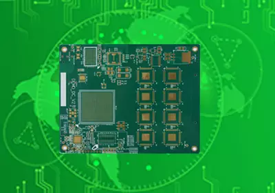
PCB testing is a critical part of electronic product development, manufacturing, equipment maintenance, and troubleshooting. It provides an effective way to identify PCB manufacturing defects, electrical faults, component failures, and functional abnormalities while ensuring stable and reliable product operation.
A standardized and comprehensive PCB testingprocess should progressively examine the board at multiple levels, including its physical condition, electrical characteristics, components, signal integrity, and functional performance. This layered approach helps reduce defect rates, shorten troubleshooting time, and improve overall manufacturing and maintenance efficiency.
Visual Inspection
Before performing any electrical measurement or powering up a PCB, a comprehensive visual inspection must be completed. Technicians should never begin testing by immediately connecting a multimeter or applying power to the board. Many basic PCB faults can be identified through visual inspection alone, making this a low-cost and highly efficient first step in the testing process.
The entire PCB should be carefully examined for cracked or damaged components, burned or discolored areas, damaged traces, lifted or detached pads, solder bridges, solder balls, missing components, poor solder joints, oxidation, contamination, corrosion, and other visible defects. Connectors should also be inspected for physical damage, misalignment, incomplete insertion, or incorrect mating. These issues can directly affect the electrical and mechanical performance of the finished PCBA.
The component installation direction should then be verified against the PCB assembly drawing and design documentation. Polarized components, including diodes, electrolytic capacitors, LEDs, integrated circuits, and connectors, must be installed in the correct orientation. Reverse installation can result in component failure, short circuits, abnormal system behavior, or complete functional failure.
Particular attention should be given to high-risk areas, including the power input circuit, voltage regulator ICs, external connectors, high-current power components, and any components showing discoloration or signs of thermal damage. Burned components, blackened PCB surfaces, and carbonized areas are often direct indicators of overcurrent, overheating, short circuits, or severe hardware damage. Such areas should be clearly identified and subjected to further testing.
Visual inspection alone cannot determine whether a PCB meets all electrical performance requirements. However, as the first low-cost screening stage of PCB testing, it can eliminate obvious assembly and physical defects before electrical testing begins. This reduces the risk of causing secondary damage by powering up a defective board and provides a reliable foundation for subsequent electrical troubleshooting.
Basic Electrical Measurements with Power Removed
After the visual inspection confirms that there are no obvious physical defects, basic electrical measurements should be performed with the PCB completely powered off. A digital multimeter can be used to verify circuit continuity and measure resistance between critical nodes, allowing technicians to identify potential short circuits and open circuits before applying power. This unpowered testing stage is an essential part of PCB troubleshooting because it provides a relatively safe way to evaluate the basic electrical condition of the board without exposing damaged components to additional electrical stress.
One of the most important measurements is the resistance between the main power rail and ground. An unusually low resistance reading may indicate a failed capacitor, damaged semiconductor device, solder bridge, incorrectly installed component, or another fault within the power distribution network. However, a low resistance reading should not automatically be interpreted as a short circuit. Certain circuit topologies naturally present a low-impedance path between the power rail and ground, so the measured value must always be interpreted in conjunction with the schematic and the intended circuit design.
The continuity mode of a multimeter can be used to verify conductive paths such as PCB traces, fuses, jumpers, connectors, and other interconnects. If two points that should be electrically connected show an open circuit, the PCB may have a broken trace, failed via, defective solder joint, or interrupted conductive path.
Resistance measurements are useful for narrowing down the location of a PCB fault, but in-circuit measurements do not always represent the actual value of an individual component. Parallel paths and surrounding circuitry can affect the measured resistance and produce readings that differ significantly from the component's nominal specification. When an accurate component-level measurement is required, the component should be electrically isolated by lifting a lead or removing it from the PCB before testing.
Pre-Power Short-Circuit Risk Assessment
A hidden short circuit on a power rail is one of the most common causes of PCB damage during power-up. The high inrush current that occurs immediately after power is applied can rapidly destroy components, PCB traces, and other hardware. For this reason, a dedicated short-circuit risk assessment should always be performed before the board is powered.
Set the multimeter to an appropriate resistance or continuity range and systematically check the relationship between each power rail and its corresponding ground reference. For PCBs containing multiple independent voltage rails, each power domain should be tested separately whenever suitable test points are accessible. This prevents faults on one power rail from being overlooked because another rail appears normal.
Test results must always be interpreted in the context of the circuit schematic. An electrolytic capacitor on a power rail may initially appear almost shorted because it charges through the multimeter probes. Semiconductor PN junctions and other low-impedance power paths can also produce readings that appear abnormal when evaluated without considering the circuit topology. Relying solely on a multimeter reading without understanding the circuit can therefore lead to incorrect fault diagnosis.
For complex PCBs, comparison testing against a known-good board can significantly improve troubleshooting efficiency. By comparing resistance measurements at identical test points on a faulty board and a functioning reference board, technicians can identify abnormal power branches and narrow down the location of hidden short circuits more quickly.
Localized Troubleshooting and Individual Component Testing
Once the initial board-level inspection has narrowed the problem down to a specific circuit area, individual components can be tested to identify the root cause. Resistors can be measured directly to verify their resistance values, while diodes can be checked using the diode-test function of a multimeter to evaluate the condition of their PN junctions. Capacitors should first be checked for obvious short-circuit or breakdown conditions. When accurate measurements of capacitance, leakage current, ESR, or other electrical parameters are required, dedicated component-testing equipment should be used.
Discrete semiconductor devices such as transistors can also undergo basic testing with a multimeter. However, in-circuit measurements may be affected by surrounding components and parallel current paths, which can make the results difficult to interpret. If the measurement is inconclusive, lifting one component lead or removing the component from the PCB can isolate it from the rest of the circuit and provide a more reliable result.
A standard multimeter cannot fully evaluate the functional performance of an integrated circuit, so measuring every IC pin individually is generally not an efficient troubleshooting strategy. A more effective approach is to verify the IC's power and ground connections, enable signals, clock waveform, reset level, and critical input and output signals. This method is particularly useful when the PCB powers up normally but the complete system fails to perform its intended function.
Controlled Power-Up and Powered Testing
The PCB should only be powered after the complete unpowered inspection has ruled out obvious high-risk faults. A bench DC power supply with adjustable voltage and current limiting should be used whenever possible. Directly connecting a potentially defective PCB to a high-power fixed-voltage supply should be avoided because an uncontrolled fault current can cause severe secondary damage.
Set the supply voltage according to the product's rated operating requirements and configure a conservative current limit before applying power. During startup, closely monitor the current response as well as the steady-state operating current. If the power supply immediately reaches its current limit, the PCB may contain a short circuit or a serious hardware fault. Conversely, if the board draws substantially less current than expected, the problem may involve the power distribution path, voltage regulator, enable control signals, or another circuit that prevents the system from starting correctly.
Powered testing should follow a logical sequence that begins with the input power and then moves toward downstream power rails and functional circuits. First verify that the external input voltage is correct, and then measure each regulated power rail on the PCB. A normal input voltage does not guarantee that the entire power system is functioning correctly. A failed downstream regulator or abnormal power rail can still prevent the system from operating normally. On boards with multiple regulated supply rails, every rail should therefore be checked individually rather than assuming that a correct input voltage confirms the integrity of the complete power system.
Power Rail and Ground Integrity Verification
Power-related faults account for a significant proportion of PCB functional failures, making power rail and ground verification one of the most important stages of PCB testing. Each power rail should be measured against its designated ground reference to determine whether the actual voltage matches the expected operating condition.
A power rail with no output may be caused by a failed voltage regulator, blown fuse, defective switching device, broken PCB trace, incorrect enable signal, or a fault in the upstream power circuit. A power rail that is significantly higher or lower than its specified value may indicate a failed regulation loop, abnormal feedback network, excessive load, or a localized circuit fault.
The overall operating current of the equipment is also an important indicator of PCB health. Excessive current consumption may indicate a shorted or failed component, abnormal current conduction, or another hardware fault. Abnormally low current consumption may indicate that part of the circuit is not receiving power or that the system has failed to enter its normal operating state.
For complex PCB troubleshooting, all measured voltage and current values should be documented rather than relying on memory. Comparing actual measurements with the schematic, design specifications, and normal operating conditions makes the troubleshooting process more systematic and traceable while improving diagnostic accuracy.
Oscilloscope Testing for Dynamic Signals and Timing
A multimeter is suitable for measuring static parameters such as voltage and resistance, but it cannot capture the dynamic behavior of electrical signals. When a PCB fault involves clock signals, switching waveforms, communication buses, PWM signals, reset timing, or other time-dependent parameters, an oscilloscope becomes an essential PCB testing instrument.
A common troubleshooting scenario occurs when the PCB power supply is completely normal but the microcontroller fails to start executing its firmware. One possible cause is a missing or abnormal clock signal. An oscilloscope can directly determine whether the clock waveform is present and can also verify its frequency, amplitude, rise and fall characteristics, duty cycle, and overall waveform integrity against the design requirements.
The same principle applies to communication interface troubleshooting. If interfaces such as UART, SPI, I²C, USB, or Ethernet fail to communicate even though the PCB powers up normally, oscilloscope measurements and protocol analysis can help identify missing signals, incorrect timing, abnormal voltage levels, or communication sequence errors.
Oscilloscope measurements must be performed correctly. The probe bandwidth should be appropriate for the signal under test, and the probe ground connection must be handled carefully. An improperly selected probe or poorly implemented ground connection can introduce noise, distort the waveform, or even create an unintended short circuit between circuit nodes. On sensitive PCBs, incorrect probing can therefore damage the board as well as compromise the measurement results.
Bare-Board Testing Before Component Assembly
Bare-board testing is fundamentally different from testing a fully assembled PCBA and represents an important quality-control stage before component assembly. The primary purpose of bare-board electrical testing is to verify PCB fabrication quality, confirm the continuity of conductive networks, and ensure adequate electrical isolation between different nets. Detecting these defects before component placement prevents manufacturing problems from being carried into the assembly process.
The main objectives of bare-board electrical testing are to identify open circuits and short circuits within the PCB's conductive networks. Flying-probe testing is widely used for prototypes, engineering samples, and low-volume PCB production because it does not require a dedicated bed-of-nails fixture and can flexibly adapt to different test-point configurations.
Bare-board testing is particularly important for multilayer PCBs. After lamination, internal traces, buried structures, vias, plated through-holes, and inner-layer copper cannot be inspected visually. Many internal fabrication defects can therefore only be identified through electrical testing.
The test criteria should be established according to the PCB fabrication specifications, engineering drawings, and applicable industry manufacturing standards. HDI PCBs, fine-line boards, and complex multilayer constructions generally require more comprehensive electrical verification than conventional two-layer boards because their higher wiring density and more complex interconnect structures introduce additional manufacturing risks.

AOI for Soldering and Assembly Quality Control
After components have been soldered during the reflow process, automated optical inspection, or AOI, is commonly used to inspect the assembly quality of the PCBA. AOI systems use industrial cameras and image-processing algorithms to automatically verify component placement and solder-joint appearance, making AOI an important automated inspection process for high-volume PCB assembly.
AOI can identify many visible assembly and soldering defects, including missing components, component misalignment, incorrect polarity, solder bridges, insufficient solder, poor solder joints, and unsoldered connections. Because the inspection process is automated, AOI can screen large quantities of PCBAs quickly and consistently, significantly improving inspection efficiency and production quality control.
However, AOI has inherent limitations. It can only inspect areas that are optically accessible and cannot directly examine hidden solder joints underneath packages such as BGAs. AOI should therefore be treated as an important visual inspection stage rather than a replacement for electrical testing or functional testing. For complete quality assurance, it should be combined with other PCB testing methods.
X-Ray Inspection for Hidden Solder Joints
Some advanced semiconductor packages contain solder joints that are completely hidden underneath the component body. BGA packages are the most typical example because the solder balls are arranged underneath the package and are not directly visible after assembly. These hidden connections represent a significant challenge for PCB inspection and testing.
X-ray inspection provides a nondestructive method for examining hidden solder joints by penetrating the component package and PCB structure. It can reveal defects such as solder bridges, insufficient solder, solder voids, open solder joints, and component misalignment that cannot be reliably detected through visual inspection or AOI.
Whether X-ray inspection is necessary depends on the PCB design, component package technology, and manufacturing process. Conventional boards without hidden solder joints may not require routine X-ray inspection. However, complex high-density PCBAs containing BGAs or other advanced packages should incorporate X-ray inspection into the appropriate quality-control process to verify hidden solder-joint integrity.
ICT for Component-Level Electrical Testing
In-circuit testing, or ICT, is an important method for performing detailed electrical verification on assembled PCBAs. By contacting designated test points with probes, ICT equipment can evaluate the electrical condition of the board and verify a wide range of component-level parameters. Traditional ICT systems use a customized bed-of-nails fixture containing multiple spring-loaded probes, allowing many test points to be contacted simultaneously.
Depending on the equipment and PCB design, ICT can verify circuit continuity and detect a wide range of component-level defects. These include incorrect resistance or capacitance values, defective diodes, open circuits, short circuits, component parameter deviations, and incorrect component polarity or installation. A properly developed ICT program can provide much more than a simple pass/fail result and can identify abnormal circuit nodes or specific defective components, significantly reducing troubleshooting time.
The major limitation of ICT is test accessibility. The PCB must provide sufficient test pads and accessible test points during the design stage, and conventional ICT systems generally require a dedicated fixture. ICT is therefore particularly suitable for mature products with stable designs and high production volumes. For engineering prototypes or products that undergo frequent design revisions, the cost and lead time associated with dedicated fixtures can make traditional ICT less economical.
Flying-Probe Testing for Prototypes and Low-Volume Production
Flying-probe testing uses multiple movable probes to contact PCB test points sequentially. Unlike conventional ICT, it does not require a dedicated bed-of-nails fixture, which makes it particularly suitable for prototypes, new product introduction, engineering validation, and low-volume PCB production.
Because the probes can be repositioned through software, flying-probe test programs can be adapted relatively quickly when the PCB design changes. This eliminates the need to manufacture a new dedicated fixture for every board revision and can substantially reduce testing costs during product development.
The primary disadvantage of flying-probe testing is its relatively low throughput. The probes contact test points sequentially rather than contacting a large number of points simultaneously, so the test cycle is generally longer than that of a conventional ICT system. For high-volume manufacturing, this difference in throughput can become significant.
The choice between flying-probe testing and ICT should therefore consider production volume, product revision frequency, test-point distribution, required test coverage, fixture cost, and test time per board. The appropriate solution should balance testing efficiency, coverage, flexibility, and total manufacturing cost.
FCT for Functional Verification
Electrical testing and component-level measurements can confirm whether the PCB has been assembled correctly, but they cannot fully determine whether the completed product performs its intended system-level functions. Functional circuit testing, commonly referred to as FCT, addresses this requirement by operating the assembled PCB under defined conditions and verifying its actual functional performance.
During FCT, the PCB is powered and operated under controlled conditions while the test system verifies power-rail behavior, overall current consumption, communication interfaces, firmware operation, digital I/O, analog signal paths, sensors, displays, motors, relays, and other product-specific functions. This allows the test process to evaluate whether the assembled PCB performs correctly within the complete system environment.
Passing ICT does not necessarily mean that the product is fully functional. A PCB may have correct component values and complete electrical continuity while still suffering from firmware startup failures, communication errors, timing problems, or other system-level faults. ICT primarily verifies electrical and assembly integrity at the component and circuit level, whereas FCT verifies whether the intended product functions are actually achieved. The two testing methods therefore complement each other and should be used together when the product requires comprehensive test coverage.
Firmware and Communication Interface Testing
Modern intelligent PCBAs commonly integrate microcontrollers, processors, memory devices, communication peripherals, and programmable logic devices. Hardware electrical testing alone cannot identify every software-related or hardware-software interaction problem, so dedicated firmware and communication interface testing is often required.
The test process should verify that the correct firmware version has been programmed into the device and that the processor can successfully complete the expected boot and initialization sequence. Communication interfaces such as UART, SPI, I²C, USB, CAN, and Ethernet should be tested using defined commands or communication sequences, with the response data checked against the expected results.
A PCB can still fail at the system level even when its power supply, solder joints, and basic electrical characteristics are normal. Incorrect firmware, abnormal configuration parameters, clock timing deviations, incompatible communication timing, or hardware-software integration problems can all prevent the system from functioning correctly. In mass production, these tests should therefore be incorporated into standardized acceptance criteria rather than relying on subjective manual judgment.
Signal Integrity Testing for High-Speed PCBs
High-speed PCBs, RF and microwave boards, and communication baseband boards cannot be fully qualified through basic continuity and DC voltage measurements alone. Signal integrity testing is required to evaluate whether high-speed signals maintain acceptable electrical characteristics as they propagate through PCB traces, vias, connectors, and other interconnect structures.
Depending on the application and required bandwidth, engineers may use high-performance oscilloscopes, vector network analyzers, time-domain reflectometers, and other specialized instruments to investigate impedance discontinuities, signal reflections, insertion loss, crosstalk, attenuation, and other high-frequency issues.
Basic continuity testing only confirms that an electrical path exists. It does not demonstrate that the path can transmit a high-speed signal with acceptable signal integrity. A PCB can therefore pass basic electrical testing and still contain serious high-frequency transmission problems. Dedicated signal integrity testing is necessary when high-speed performance is a critical design requirement.
PCB Reliability Testing
For PCBs used in automotive electronics, aerospace, medical equipment, industrial control systems, and other high-reliability applications, conventional electrical and functional testing at room temperature is not sufficient to verify long-term performance. Reliability testing is required to evaluate whether the PCB can maintain stable operation under the environmental and mechanical stresses expected during its service life.
Typical reliability testing may include temperature cycling, damp heat testing, thermal shock, random vibration, and other environmental or mechanical stress tests. The specific test conditions should be selected according to the actual application environment, product reliability requirements, material system, and applicable industry standards.
Routine production testing generally determines whether an individual finished PCB meets its electrical and functional specifications at the time of shipment. Reliability testing serves a different purpose by evaluating the long-term stability of the PCB design and manufacturing process and identifying potential degradation or latent failure mechanisms under prolonged stress. Compared with conventional consumer electronics, PCBs used in automotive, aerospace, medical, and other high-reliability applications typically require more rigorous and comprehensive reliability validation.
Selecting the Appropriate PCB Testing Method
There is no single PCB testing method that can identify every type of defect. Each testing technique has a specific purpose and inherent limitations. Visual inspection is effective for identifying physical and assembly defects but cannot reliably detect hidden electrical faults. A multimeter is useful for basic electrical measurements but cannot analyze dynamic signals. AOI is highly effective for visible soldering and placement defects but cannot inspect hidden solder joints beneath packages. X-ray inspection can evaluate concealed solder connections but cannot determine firmware or system functionality. ICT provides detailed component-level electrical verification but depends heavily on PCB test-point accessibility. FCT verifies system-level functionality but generally provides less precise fault localization than dedicated electrical test systems.
A mature PCB testing strategy should therefore use multiple complementary methods rather than relying on a single inspection or test process. The testing sequence should also follow the principle of performing lower-cost screening before more expensive and time-consuming verification. Obvious assembly and manufacturing defects should be eliminated as early as possible so that defective boards do not proceed unnecessarily into system assembly or advanced functional testing. This approach helps control testing costs while improving overall quality-control efficiency.
Design for Testability in PCB Design
PCB testability should not be treated as a problem to be solved only during manufacturing or after a product fails. It should be incorporated into the PCB design process from the beginning through design for testability, or DFT. Proper DFT planning can reduce testing difficulty, increase test coverage, and make future troubleshooting more efficient.
During PCB design, dedicated test pads should be provided to give test probes reliable physical access to important electrical nodes. Critical power rails and signal networks should be arranged with test accessibility in mind, making it easier to perform debugging, electrical verification, and fault isolation during production and maintenance.
A complete DFT strategy should define testing requirements before PCB layout is finalized. Engineers should identify which signals need external access, determine where probes can physically contact the board, and consider the requirements of ICT or flying-probe testing. FCT requirements should also be defined in advance so that the necessary system-level functions can be verified after assembly.
For high-density PCB designs, testability must be balanced against routing density, component placement, mechanical constraints, thermal requirements, and electrical performance. A board may be electrically functional from a design perspective but still become difficult and expensive to test if adequate test access is not considered during layout. Integrating DFT into the design process helps prevent such problems and supports more efficient volume manufacturing.
PCB testing is a systematic process that extends across PCB design, fabrication, assembly, quality control, maintenance, and repair. By combining visual inspection, unpowered electrical measurements, controlled power-up, component-level testing, AOI, X-ray inspection, ICT, flying-probe testing, FCT, firmware verification, signal integrity analysis, and reliability testing, engineers can progressively identify different categories of PCB defects and distinguish between manufacturing defects, hardware failures, and software-related problems.