Share cost-effective products and high-quality services with customers. Contact Us


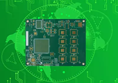
PCB wiring is one of the most fundamental and critical processes in printed circuit board (PCB) design. It specifically refers to the process of planning and routing conductive copper traces across the board to establish electrical connections between all electronic components. Traditional circuit assembly relied on individual wires that were manually soldered to connect components.
PCB wiring has effectively replaced this cumbersome approach by integrating precisely designed copper traces into the outer and inner layers of the circuit board, creating a reliable network for signal transmission and power delivery. As a result, PCB wiring serves as a core foundation for implementing circuit functions in electronic products.
In a standard printed circuit board structure, various electronic components, including resistors, capacitors, integrated circuits (ICs), connectors, diodes, and transistors, are mounted and soldered onto designated metal pads on the PCB. The primary function of PCB wiring is to follow the electrical logic defined by the circuit schematic and connect these individual pads in an organized manner using continuous copper traces.
Depending on the functional requirements of the product and the complexity of the circuit, PCB routing can be implemented on single-layer, double-layer, or multilayer boards. Simple low-voltage and low-frequency circuits often use single-layer or double-layer PCBs, with traces routed primarily on one or both sides of the board. In contrast, complex circuits used in high-end precision equipment and high-speed intelligent devices typically employ multilayer PCBs, where traces are distributed across multiple internal layers to maximize space utilization and reduce the overall board footprint.
For multilayer PCBs, electrical connections between different layers are commonly achieved using vias. Plated-through vias and other types of vias provide vertical electrical connectivity between PCB layers, allowing traces on the outer layers to connect efficiently to inner-layer circuitry and enabling interconnection between different regions of internal copper layers. This multilayer interconnection capability makes high-density and compact PCB layouts possible while effectively addressing the routing congestion and limited board space associated with complex electronic circuits. It is also a critical technological foundation for developing smaller, lighter, and more highly integrated electronic products.

The quality of PCB routing directly affects the overall electrical performance, operational stability, service life, and manufacturability of the circuit board. It is a critical link between theoretical circuit design and industrial-scale PCB manufacturing. During the routing process, professional PCB designers must balance a wide range of parameters and design considerations, including trace width, trace spacing, copper thickness, current-carrying capacity, signal integrity, power distribution, grounding strategy, electromagnetic interference (EMI) suppression, thermal management, and manufacturing tolerances. An inappropriate design decision in any of these areas can potentially result in circuit failures or manufacturing defects.
In practical PCB design, routing parameters should be tailored to the electrical characteristics and functional requirements of each circuit. The fundamental principle is to adopt a zoned and application-specific routing strategy. High-current power circuits require wider copper traces and, where necessary, thicker copper layers to reduce trace resistance and prevent excessive voltage drops, localized heating, and potential trace damage during operation.
By contrast, low-level analog signals and high-speed signals require more precise routing control. Their routing paths, trace lengths, geometry, spacing, and layer transitions must be carefully managed to minimize crosstalk and electromagnetic interference while maintaining signal integrity and transmission accuracy during high-speed data transfer. At the same time, adequate clearance must be maintained between conductive features in accordance with applicable design rules to prevent short circuits and other manufacturing defects, thereby improving PCB production yield and reliability.
In PCB design, the concepts of PCB wiring,PCB routing, and PCB layout are closely related but have distinct meanings and should not be treated as interchangeable terms. They represent different levels of the overall PCB design process. PCB wiring primarily refers to the resulting copper-trace network that provides the physical electrical connections between components and circuit nodes.
PCB wiring refers to the actual design process of determining the paths, directions, and layer assignments of those traces, typically with the assistance of electronic design automation (EDA) software. PCB layout is the broader, system-level physical design process that encompasses component placement, overall routing strategy, via placement, copper pours and planes, grounding design, board outline definition, keep-out areas, and other physical design considerations. In this sense, PCB layout serves as the top-level design framework that incorporates both routing and wiring.
A scientifically designed and properly engineered PCB routing strategy not only provides stable signal interconnections and efficient power delivery between components but also makes optimal use of the limited available board space. It can improve the thermal performance of the overall assembly, reduce electromagnetic interference, and enhance the operational stability and service life of the finished electronic product.
Conversely, poor routing can lead to a range of hardware problems, including excessive voltage drops, signal distortion, data transmission errors, localized thermal hotspots, and low manufacturing yields. In severe cases, inadequate routing can result in short circuits, complete system malfunction, or functional failure, significantly increasing both product development and manufacturing costs.
PCB wiring is the essential process that transforms an abstract circuit schematic into a physical circuit board that can be manufactured, assembled, and operated reliably. As industries such as consumer electronics, industrial automation, new energy, and semiconductors continue to develop rapidly, electronic products are evolving toward greater miniaturization, thinner form factors, higher operating speeds, and higher component density. As a result, circuit architectures are becoming increasingly sophisticated and complex, placing higher demands on PCB layout and routing technology.