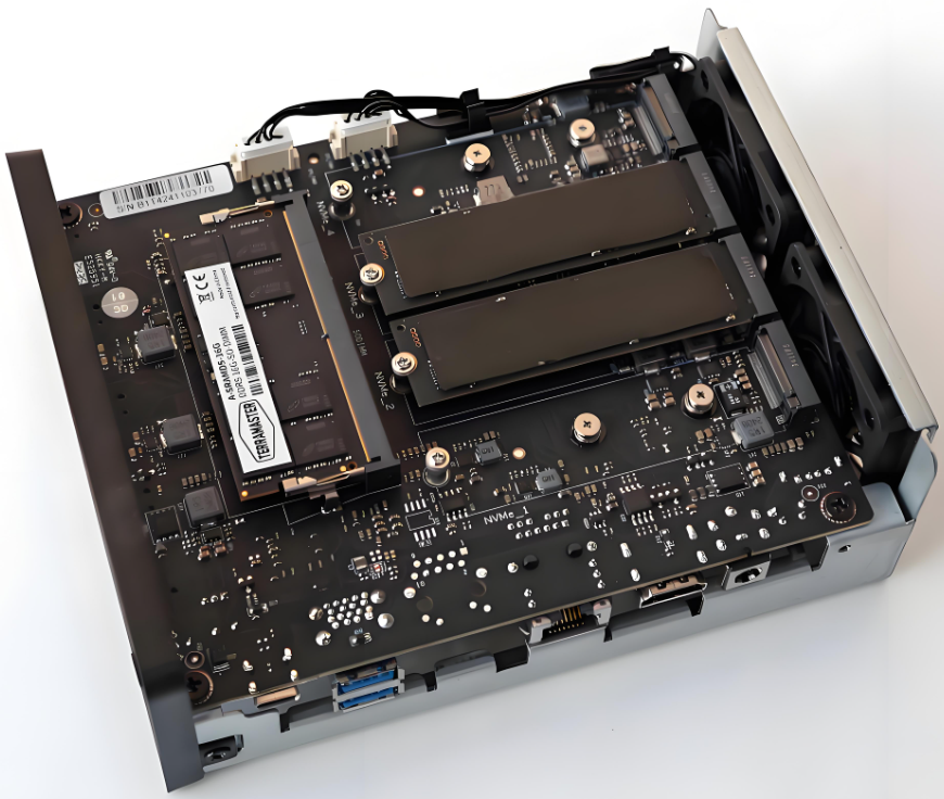
In today's digital landscape, Solid-State Drives (SSDs) have become the preferred storage solution due to their speed, reliability, and energy efficiency. With increasing demand for high-performance storage, developing an SSD circuit board prototype requires meticulous planning, advanced design techniques, and precise manufacturing processes. This article explores the essential aspects of SSD PCB prototyping, from component selection to fabrication and testing.

SSD PCB
Understanding the Core Components of an SSD
Before diving into the prototyping process, it's crucial to understand the key components that make up an SSD:
1. NAND Flash Memory
NAND flash serves as the primary data storage medium. Most modern SSDs use 3D NAND technology, which stacks memory cells vertically to increase density and improve efficiency. For an SSD with a storage capacity of 256-GB, multiple NAND flash chips are used in parallel to achieve the required performance and reliability.
2. SSD Controller
The controller acts as the brain of the SSD, managing data transfer, wear leveling, error correction, and communication with the host system. Popular controllers include those from Phison, Silicon Motion, Marvell, and Samsung, supporting SATA, PCIe, or NVMe interfaces.
3. DRAM Cache
Many SSDs incorporate a DRAM cache (e.g., LPDDR4 or DDR3) to temporarily store frequently accessed data, improving performance and reducing latency.
4. Power Management IC (PMIC)
Efficient power regulation is essential for SSD longevity and performance. PMICs help optimize power consumption, ensuring stable operation while minimizing heat dissipation.
5. Interface and Protocols
The SSD's performance largely depends on the chosen interface:
SATA III (6Gbps) – Suitable for budget-friendly SSDs but limited in speed.
PCIe NVMe (Gen 4/Gen 5) – Provides significantly higher data transfer rates for high-performance applications.
Prototyping the SSD Circuit Board
Once the key components are identified, the next step is designing and prototyping the SSD PCB.
1. Schematic Design
The first step is creating a detailed schematic using PCB design software such as Altium Designer, KiCad, or Cadence Allegro. This includes:
Defining power and data signal connections between components.
Implementing error correction and wear-leveling algorithms in the firmware.
Ensuring compliance with NVMe or SATA protocols for compatibility.
2. PCB Layout and High-Speed Signal Integrity
The layout design significantly impacts SSD performance and reliability. Critical considerations include:
Layer Stack-up: A 4 to 8-layer PCB is typically required for high-speed signal routing and power distribution.
Impedance Control: Differential pairs for PCIe lanes must be routed with controlled impedance to maintain signal integrity.
Thermal Management: Implementing copper pours, thermal vias, and heat sinks to dissipate heat efficiently.
Minimal Trace Lengths: Ensuring short and direct traces between the controller, NAND flash, and DRAM to reduce signal loss.
3. Material Selection
Choosing the right PCB material is crucial for performance. High-speed SSDs require low-loss laminates such as:
High-quality FR4 – Standard for cost-effective designs.
Rogers or Isola materials – For advanced PCIe Gen 4/5 SSDs requiring minimal signal attenuation.
4. Prototype Manufacturing
Once the PCB layout is finalized, a small batch of prototype boards is fabricated for initial testing. The process involves:
PCB Fabrication: High-precision etching, drilling, and plating to form multilayer boards.
Component Assembly: Using Surface Mount Technology (SMT) for precise placement of NAND flash, controllers, and passive components.
Firmware Flashing: Uploading the SSD firmware to the controller to enable proper data handling and communication.
5. Testing and Validation
Before mass production, rigorous testing is conducted to ensure reliability and efficiency:
Performance Benchmarking: Measuring read/write speeds, latency, and IOPS under various workloads.
Thermal Analysis: Ensuring the SSD operates within safe temperature ranges.
Stress Testing: Simulating real-world conditions such as high workloads and power fluctuations to assess durability.
Signal Integrity Tests: Using oscilloscopes and TDR (Time Domain Reflectometry) to validate high-speed transmission quality.
6. Iteration and Refinement
The prototyping process is rarely perfect on the first attempt. Engineers analyze test results, identify weaknesses, and refine the design by:
Optimizing firmware algorithms for better wear leveling and error correction.
Adjusting PCB trace lengths and layer stack-up for improved signal performance.
Enhancing thermal dissipation for better power efficiency.
Key Takeaways and Future Trends
Developing an SSD circuit board is a complex but rewarding process that requires a balance between hardware engineering, firmware optimization, and manufacturing precision. As the industry progresses, we can expect:
Higher-capacity NAND flash with denser 3D stacking.
PCIe Gen 5 and Gen 6 adoption for ultra-fast SSDs.
AI-driven firmware optimizations for predictive failure analysis.
By following a structured prototyping approach, engineers can create efficient, high-performance SSDs that meet the growing demands of modern computing. Whether for consumer devices or enterprise storage solutions, precision in SSD PCB design and prototyping is key to delivering next-generation performance.