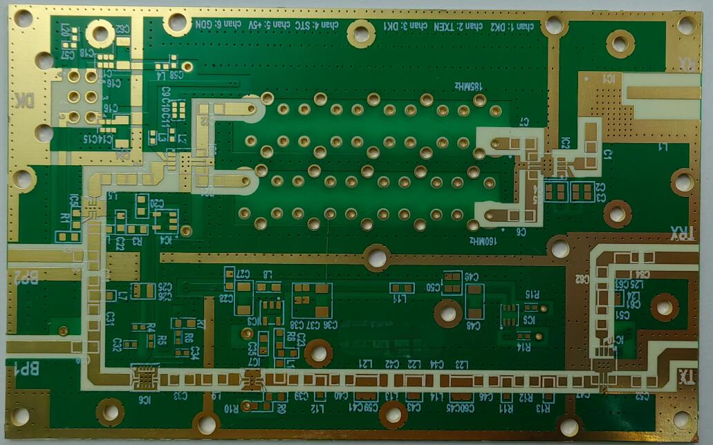
In terms of layout, when the PCB size is too large, although soldering is easier to control, the printed lines are long, impedance increases, noise resistance decreases, and costs increase; If it is too small, heat dissipation will decrease, welding will be difficult to control, and adjacent lines may interfere with each other, such as electromagnetic interference from circuit boards.
Therefore, it is necessary to optimize the PCB board design
1. Shorten the wiring between high-frequency components and reduce EMI interference.
2. For heavy components exceeding 20g, they should be fixed with brackets and then welded.
3. Heating elements should consider heat dissipation issues to prevent defects and rework caused by large Δ T on the surface of the element. Thermal sensitive elements should be kept away from the heat source.
4. The arrangement of components should be as parallel as possible, which is not only aesthetically pleasing but also easy to weld, making it suitable for large-scale production. The optimal design for the circuit board is a 4:3 rectangular shape. Do not have sudden changes in wire width to avoid discontinuity in wiring. When the circuit board is heated for a long time, the copper foil is prone to expansion and detachment, therefore, the use of large-area copper foil should be avoided.

PCB
When digital and analog circuits share the same components on the same board, the layout and wiring of the circuit must be carefully designed:
Consider separate analog and digital power supplies.
Understand all return paths.
Although expensive, if possible, please use a four layer circuit board.
Do not wire analog signals in parallel with clocks or fast digital signals.
If analog and digital signals must intersect, make sure these signals intersect at 90 degrees to minimize coupling capacitance.
The power layer should appear in the corresponding area of its signal line. For example, running only analog signals on the analog power layer.
Place the bypass capacitor as close as possible to the IC. In addition, it is necessary to ensure that the bypass connection of the power signal is low impedance.
If possible, please use independent analog and digital signals as well as independent digital and analog components on the circuit board. Specify the "Analog" and "Digital" areas of the PCB board.
Long wiring should be avoided for high impedance input signals, otherwise it will couple noise into the signal link like an antenna.
Expand the width of the power supply wiring as much as possible to reduce impedance.
Place the analog signal closest to the ground plane to minimize inductive crosstalk.
When connecting power signals between layers, please use large or multiple vias to reduce impedance.
Minimize the digital rise and fall time of digital signals as much as possible.
Use protective wires to isolate analog and digital signals from each other.
The above shares some tips for optimizing PCB board design and the layout and wiring of circuits must pay attention to methods