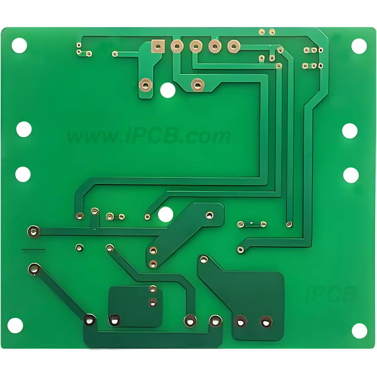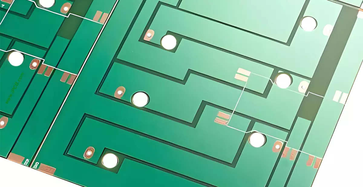
Product Name: Single Layer PCB
Material: FR-4, CEM-1, CEM-3
Quality standard: IPC 6012
Layers: 1 layer PCB
Thickness: 0.6mm-1.6mm
Copper thickness: 0.5-1oz
Surface technology: OSP, HASL
Solder mask: Green, Blue, Black, White
Screen printing: Black, White
Application: Electronic Products
The components of a single layer PCB is concentrated on one side, while the circuit wires are concentrated on the other side. Because wires only appear on one side of a single layer PCB, we call this type of PCB a single layer PCB or 1-layer PCB. Because single layer PCB have many strict limitations in designing circuits, as there is only one layer of circuit, the wiring cannot intersect and must follow separate paths.
Single layer PCB is a circuit board with only one side attached with conductive patterns. The manufacturing process of single layer PCB is simple, and the cost of single layer PCB is relatively low, so it still has applications in some electronic products with strict cost requirements. For example, some simple electronic toys, calculators, remote controls, etc., due to their relatively single functions, do not have high requirements for circuit boards, so single layer PCB have become the ideal choice for these products.
The cost of a single layer PCB circuit board has multiple aspects, including the cost of raw materials, production costs, production processes, special requirements, etc. The actual pricing needs to be negotiated with the single layer PCB supplier. The general unit price calculation formula is: (length MM) x (width MM) x 0.01 x unit price (yuan/square meter) ÷ 10000 (rounded to three decimal places)

Single layer PCB production process
Single sided copper-clad board ->cutting ->(brushing, drying) ->drilling or punching ->screen printing anti etching graphics or using dry film ->curing inspection and board repair ->etching copper ->removing anti etching printing materials, drying ->brushing, drying ->screen printing solder mask graphics (commonly green oil), UV curing ->screen printing character marking graphics, UV curing ->preheating, punching and appearance ->electrical opening and short circuit testing ->brushing, drying ->pre coating solder aid anti oxidation agent (drying) or spray tin hot air leveling ->inspection and packaging ->single layer PCB finished products leaving the factory
Single layer PCB material
Single layer PCB printing is generally made of copper-clad laminates, with copper foil laminates being commonly used. When selecting boards, consideration should be given to electrical performance, feasibility, processing technology requirements, economic indicators, and other aspects. Commonly used copper-clad laminates include copper-clad phenolic paper laminates, copper-clad epoxy paper laminates, copper-clad epoxy glass cloth laminates, copper-clad epoxy phenolic glass cloth laminates, copper-clad polytetrafluoroethylene glass cloth laminates, and epoxy glass cloth for multilayer printed circuit board.
Phenolic paper substrate (cardboard, plywood, V0 board, flame retardant board, red lettered copper-clad laminate, 94V0). The most commonly used product models for phenolic paper-based copper-clad laminates are FR-1 (flame retardant) and XPC (non flame retardant). Single sided copper-clad laminates can be easily judged by the color of the characters on the back of the board. Generally, red letters are FR-1 (flame retardant type), and blue letters are XPC (non flame retardant type). This type of board is relatively the cheapest compared to other types of boards.
Epoxy fiberglass cloth substrate (epoxy board, fiberglass board, fiberboard, FR4) is made of epoxy resin as an adhesive. A type of substrate reinforced with electronic grade fiberglass cloth. Its adhesive sheet and inner core thin copper-clad laminate. It is an important substrate for making multilayer printed circuit board. The working temperature is relatively high. The performance itself is less affected by the environment. In terms of processing technology. Compared to other resin based fiberglass cloth substrates, it has significant advantages. This type of product is mainly used for double sided PCB. Compared to phenolic paper substrates, it is about twice as expensive, with a commonly used thickness of 1.5mm.
Composite substrate (CEM-1 board, also known as 22F in some parts of China) mainly refers to CEM-1 and CEM-3 composite based copper-clad laminates. Using wood pulp fiber paper or cotton pulp fiber paper as the core material reinforcement material. Using fiberglass cloth as the surface reinforcement material. Both are copper clad laminates made of flame-retardant epoxy resin. It is called CEM-1. Using fiberglass paper as the core material reinforcement material. Using fiberglass cloth as the surface reinforcement material. All immersed in flame-retardant epoxy resin. Made of copper-clad laminates. It is called CEM-3. These two types of copper-clad laminates are the most common composite based copper-clad laminates. This type of board is cheaper than FR4 type board.

single layer PCB circuit board
Although single layer PCB board still have market demand in certain fields, they also face significant challenges. On the one hand, with the increasing complexity of electronic product functions, the requirements for circuit board is also becoming higher, and high-end PCB board products such as multilayer PCB and HDI PCB board are gradually becoming mainstream in the market. On the other hand, the increasingly strict environmental regulations have also put forward certain restrictions on the production and use of single layer PCB.
Although single layer PCB are no longer the forefront PCB products in the industry in terms of technology, they still have irreplaceable value in specific markets and application scenarios.
Product Name: Single Layer PCB
Material: FR-4, CEM-1, CEM-3
Quality standard: IPC 6012
Layers: 1 layer PCB
Thickness: 0.6mm-1.6mm
Copper thickness: 0.5-1oz
Surface technology: OSP, HASL
Solder mask: Green, Blue, Black, White
Screen printing: Black, White
Application: Electronic Products
iPCB Corporation provides support for PCB Prototype and Electronic Manufacturing. You can request consultation or quotation for PCB, PCBA and ODM here, please contact email: sales@ipcb.com
We will respond very quickly.