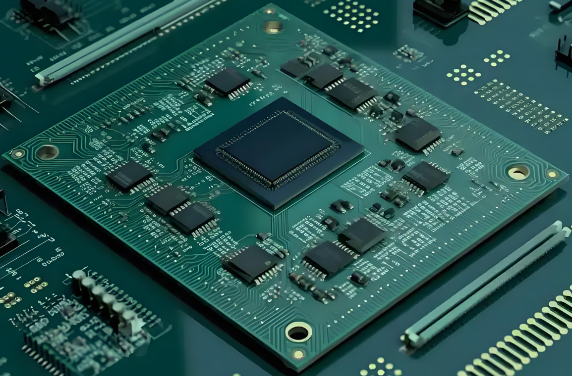
The electronic industry is increasingly focused on High-Density Interconnect boards, a trend driven by the demand for compact devices. HDI technology is essential for optimizing circuit designs in increasingly miniaturized form factors. One key question arises in this context: Are HDI boards economical? At IPCB, we will explore this question from various dimensions and conclude that HDI boards can indeed be a cost-effective solution. Let's examine the supporting arguments.

HDI PCBs
Layers and Laminations: A Cost-Benefit Perspective:
While it's true that boards with multiple layers and laminations typically have a higher initial cost compared to single-layer alternatives, the overall economic impact must consider various factors. For instance, increasing the number of layers can lead to smaller board sizes a crucial advantage in today's tightly packed devices.
When assessing the cost efficiency of HDI boards versus conventional designs, it is essential to evaluate the design complexities, yield rates, and manufacturing capabilities of your PCB partner. A designer might prefer blind and buried vias with an 8-mil hole-to-copper clearance over an HDI board utilizing a 3-4 mil clearance and fewer layers. However, the overall manufacturing yield and associated costs often dictate the final choice.
The capabilities of your PCB manufacturer are a vital consideration. If a manufacturer specializes in prototyping rather than mass production, the risk of wastage and increased costs can rise significantly. For example, while a manufacturer may successfully produce ten units of a six-layer design with a 3-mil clearance, scaling up to 10,000 boards may lead to substantial price increases due to inefficiencies, potentially surpassing 50%.
The Necessity of HDI Technology:
HDI technology shines in applications demanding high-density component placements, such as Ball Grid Arrays (BGAs) in tight pitches. Conventional designs could achieve similar results through smaller drilled holes, but this approach often results in low yields due to fabrication complexities.
Conversely, HDI designs simplify these challenges. With trace widths of just 2.5 mils to 3 mils in crucial areas and wider traces of 4-5 mils elsewhere, manufacturers can reduce the total number of layers while ensuring performance and manufacturability.
Creating economically viable HDI boards often benefits from collaborative discussions with manufacturing partners, who can provide insights on best practices and materials.
Material Selection for Cost Efficiency:
The material chosen for HDI boards significantly affects production costs. While designers can reference data sheets for material performance, the actual costs associated with board fabrication can vary widely. Identifying materials that satisfy both electrical and mechanical specifications while remaining economically viable requires expert insights from manufacturing partners.
An experienced manufacturer can recommend materials that not only fulfill performance criteria but also enhance ease of manufacturability. This approach fosters a balanced trade-off between performance and production cost, maximally benefiting the end product.
Materials with properties conducive to dimensional stability and laser drilling resilience, alongside appropriate thermal management, are essential for high-quality HDI boards. The selection of materials with low dissipation factors and stable dielectric constants can further enhance signal integrity, ultimately promoting faster signal propagation without distortion.
Critical Factors in HDI PCB Fabrication
For cost-effective HDI board manufacturing, three fundamental material characteristics are paramount:
Dimensional Stability: Predictable behavior during the heating and laminating process minimizes waste and defects.
Machinability: The material must withstand precise laser drilling processes, ensuring quality and throughput.
Durability: The capability to endure the stresses of multiple laminations during production is essential for multi-layer boards.
Understanding the nuances of laser drilling often better described as a vaporization process erves as a critical factor in material selection. Variability in how different materials absorb laser energy can drastically impact manufacturability.
The Role of Resins in Manufacturing:
Epoxy resin is the most commonly utilized material in HDI boards due to its favorable mechanical, electrical, and thermal properties, as well as its exceptional adhesion characteristics. However, its flammability poses challenges, especially in high-density applications that generate considerable heat. Incorporating flame-retardant additives or transitioning to BT-Epoxy resins in certain environments can mitigate this risk.
The Economic Impact of Via Types:
The overall cost and quality of HDI boards are heavily influenced by via quality and plating methods. Mechanical and laser drilling are the primary techniques employed. Although mechanical drilling is traditionally perceived as more economical for singular applications, laser drilling typically outperforms in large-scale, high-precision tasks due to lower operational costs when considering extensive production runs.
Conclusion:
The path to economically producing HDI boards encompasses a tapestry of factors, including material selection, yield optimization, and drilling methodologies. By leveraging 3-mil traces and effective drilling mechanisms, higher yield rates can be achieved while minimizing the number of required PCB layers.
IPCB strongly advocates for collaborative discussions with your manufacturing partner throughout the design process. This partnership can illuminate the optimal materials and manufacturing strategies, striking an ideal balance between cost, performance, and manufacturability.
By understanding these dynamics, businesses can make informed decisions that not only meet their design specifications but also adhere to budget considerations, ultimately leading to successful product outcomes.