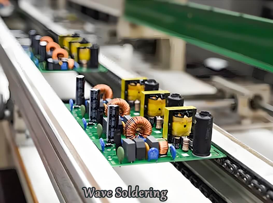
Wave soldering is to make the soldering surface of the plug-in board directly contact with high-temperature liquid tin to achieve the purpose of soldering. The high-temperature liquid tin maintains an inclined surface, and a special device makes the liquid tin form a wave-like phenomenon, so it is called "wave soldering". Its main material is solder bar. This article mainly introduces the content of wave soldering tinning. First, it introduces the phenomenon of wave soldering tinning, then introduces the reasons for wave soldering tinning, and finally explains the wave soldering tinning removal technology and how to reduce wave soldering tinning.
Wave soldering tinning phenomenon
1. The tinning phenomenon is caused by the excessive length of the component pins when the circuit board is wave soldered. When pre-processing the component pins, please note that the extended length of the general component pins is 1.5-2mm. If it does not exceed this height, this undesirable phenomenon will not occur.
2. As the circuit board process design becomes more and more complex, the lead pin spacing becomes denser and denser, resulting in the phenomenon of tinning after wave soldering. Changing the pad design is a solution. For example, reducing the pad size, increasing the length of the pad exiting the wave side, increasing the flux activity/reducing the lead extension length are also solutions.
3. After wave soldering, the molten tin infiltrates the surface of the circuit board, forming a phenomenon of tin connection between the pins of the components. The main reason for this phenomenon is that the inner diameter of the pad is too large, or the outer diameter of the pin of the component is too small.
4. The dense-footed components are densely packed in one area, resulting in the tin connection of the component feet after wave soldering.
5. Wave soldering tinning caused by oversized pads.
6. Tinning phenomenon of component pins after wave soldering due to poor solderability of component pins.

Wave Soldering
What is the reason for Wave soldering?
1. The flux is not active enough.
2. The wettability of the flux is not enough.
3. The amount of flux applied is too small.
4. The flux is not applied evenly.
5. The circuit board cannot be coated with flux in some areas.
6. The circuit board is not tinned in some areas.
7. Some pads or solder feet are severely oxidized.
8. The wiring of the circuit board is unreasonable (the distribution of components is unreasonable).
9. The board running direction is wrong.
10. The tin content is not enough, or the copper content exceeds the standard; [Excessive impurities cause the melting point (liquidus) of the tin liquid to rise]
11. The foaming tube is blocked and the foaming is uneven, resulting in uneven coating of the flux on the circuit board.
12. The wind knife setting is unreasonable (the flux is not blown evenly).
13. The board running speed and preheating are not well coordinated.
14. Improper operation method when hand tinning.
15. The chain inclination is unreasonable.
16. The wave peaks are uneven.
Wave soldering tin removal technology
There are also many advanced supplementary options within each machine type. For example, it provides a patented hot air knife bridging technology, which is used to remove bridges and conduct damage stress testing of solder joints. The air knife is located at the exit of the welding tank and shoots 0.4572mm narrow hot air towards the solder joint at an angle of 40° to 90° to the horizontal. It allows all the perforated solder joints that were not soldered well enough due to the air left in the first time to be refilled with solder without affecting the normal solder joints. However, it must be noted that in order to significantly improve the quality of solder joints, it is not necessary to set more options on the wave soldering equipment. And for all production equipment, it is also important to check the true accuracy of each engineering data. A good way is to run the board on the machine before buying.
How to reduce Wave soldering bridging
1. Design according to PCB design specifications. The long axis of the two end chips is perpendicular to the welding direction, and the long axis of SOT and SOP should be parallel to the welding direction. Widen the pad of the pin after SOP (design a tin stealing pad)
2. The pins of the plug-in components should be formed according to the hole spacing and assembly requirements of the printed circuit board. If a short plug-in soldering process is used, the pins of the soldering surface components are exposed 0.8~3mm from the surface of the printed circuit board, and the component body is required to be straight when plugged in.
3. Set the preheating temperature according to the PCB size, whether it is a multi-layer board, the number of components, and whether there are mounted components.
4. The tin wave temperature is 250±5℃, and the welding time is 3~5s. When the temperature is slightly lower, the conveyor belt speed should be slowed down.
5. Replace the flux.
Wave soldering tinning is primarily caused by excessive solder exposure during the process, leading to undesirable solder build-up on components. To reduce tinning, manufacturers can optimize parameters such as solder temperature, conveyor speed, and preheating time. Additionally, using appropriate flux types and maintaining a clean solder bath can significantly minimize the risk of tinning. By implementing these strategies, companies can enhance the reliability of their soldered joints and improve overall product quality.