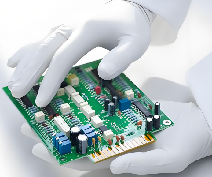
PCB prototyping is a fundamental step in the electronics development process, enabling engineers to evaluate design concepts, detect potential flaws, and refine performance before full-scale production. By investing in prototyping, manufacturers can prevent costly errors, enhance reliability, and ensure compliance with industry standards. This phase plays a crucial role in optimizing functionality, durability, and overall design efficiency, making it indispensable in modern electronic manufacturing.

PCB Prototype
Key Stages in the PCB Prototyping Process
1. Schematic Design
The prototyping journey begins with translating conceptual ideas into a structured schematic using PCB design software. This schematic serves as a blueprint, defining components, electrical connections, and functionality. A well-drafted schematic minimizes errors and streamlines subsequent design steps.
2. PCB Layout Design
Once the schematic is finalized, designers create the physical layout of the PCB. This involves placing components strategically and routing electrical traces while considering signal integrity, thermal management, and electromagnetic interference. A meticulously designed layout ensures manufacturability and optimal circuit performance.
3. Selection of Materials and Components
Choosing the right materials and components is essential to the prototype's performance. Factors such as thermal stability, electrical properties, and mechanical strength influence material selection. Additionally, sourcing components with consideration for availability, cost, and long-term viability is vital for a seamless transition to mass production.
4. Prototype Fabrication
After finalizing the layout, the design is sent to a PCB prototype manufacturer. This stage involves fabrication techniques such as etching, drilling, plating, and applying solder masks. Producing a limited batch of prototypes allows for testing and validation without committing to full-scale production.
5. Assembly and Soldering
Following fabrication, the next step is component assembly and soldering. Depending on complexity, this process can be performed manually for low-volume prototypes or through automated methods such as Surface Mount Technology (SMT) for higher precision and efficiency.
6. Testing and Debugging
With the prototype assembled, rigorous testing is conducted to assess functionality, electrical performance, and adherence to design specifications. This phase identifies potential issues such as signal interference, power inefficiencies, and component failures, enabling designers to make necessary adjustments.
7. Iterative Refinement
The prototyping process often requires multiple iterations. Insights gained from testing are incorporated into revised designs, leading to improved versions of the PCB. This iterative approach enhances performance, reliability, and manufacturability, ensuring the final design is production-ready.
Best Practices for Successful PCB Prototyping
Comprehensive Design Review: Conducting in-depth design reviews before prototyping minimizes errors and reduces revisions.
Efficient Component Sourcing: Ensuring the availability of key components prevents production delays and cost overruns.
Collaboration with Manufacturers: Maintaining clear communication with PCB fabricators ensures alignment with design specifications and quality standards.
Thorough Testing Protocols: Implementing extensive testing procedures ensures prototypes meet functional and regulatory requirements.
Conclusion
PCB prototyping is a critical phase in electronic product development, bridging the gap between theoretical designs and functional hardware. By embracing a structured prototyping process, engineers can refine their designs efficiently, reduce production risks, and accelerate time-to-market. Whether for consumer electronics, automotive applications, or industrial devices, mastering PCB prototyping is key to achieving innovation, reliability, and success in the ever-evolving electronics industry.