Introduction
Printed circuit boards (PCBs) form the backbone of nearly all modern electronic devices and orchestrate the complex electronic dance that powers our technology-driven world. Amid a complex web of copper traces and components, printed circuit boards serve as the humble yet integral element that brings together the physical world of components and the abstract world of electrical connections. These discrete copper patches play a vital role in ensuring reliable signal transmission, efficient power flow, and stable component anchoring.
In this article, we embark on a journey to discover the often-overlooked importance of printed circuit boards, delving into their various types, design complexities, and the critical role they play in the world of electronic design and manufacturing.
Types of PCB Pads
PCB pads come in a variety of shapes and sizes, each tailored for specific components and applications. The most common types of PCB pads are discussed in detail below:
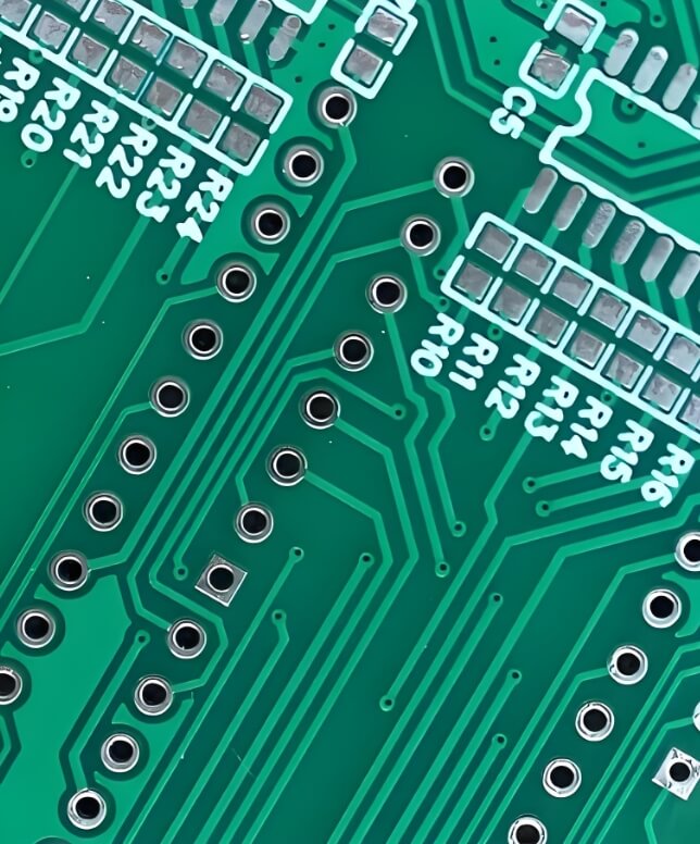
Through-hole pads
These are the classic round or oval pads that fit through-hole components like resistors, capacitors, and diodes. They are often used for components that require a strong mechanical connection to the PCB. PCB through-hole pads are fundamental and durable components in electronic design, acting as a critical connection between the component and the conductive path of the printed circuit board (PCB). With a round or oval shape, these pads play a key role in mounting the leads of through-hole components such as resistors, capacitors, diodes, and connectors. Through-hole technology has long been a cornerstone of electronic assembly, providing a strong mechanical connection and facilitating assembly and repair. The design and configuration of through-hole pads directly impact soldering quality, component stability, and the overall integrity of the PCB assembly.

Through Hole Pads
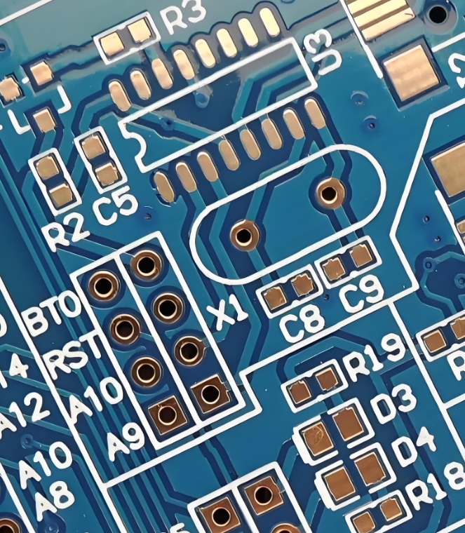
Surface Mount Pads
Surface mount technology (SMT) pads are smaller and allow components to be soldered directly to the surface of a PCB. Available in a variety of shapes, including rectangular, oval, and custom designs, these pads are an integral part of modern compact electronics. These carefully designed and strategically placed pads serve as the hub of the surface mount technology (SMT) process. Made of conductive material, usually copper, these pads provide the foundation for soldering a wide range of electronic components, from tiny resistors to complex integrated circuits. Their geometries vary to accommodate specific components, with pads for secure bonding and electrical connections, component pads customized for different surfaces, and thermal pads for efficient heat dissipation.
The design of these pads requires a delicate interplay of factors: pad size, shape, spacing, and solder mask considerations all work in harmony to ensure optimal soldering and tight connections. In an age of ever-increasing technological advancement, surface mount printed circuit boards are the unsung heroes that have enabled the miniaturization of devices, the orchestration of complex circuits, and the manifestation of innovation. As electronics continue to evolve, the humble printed circuit board remains the cornerstone of modern electronics manufacturing, uniting the worlds of design, engineering, and functionality with remarkable precision and skill.

Surface Mount Pads
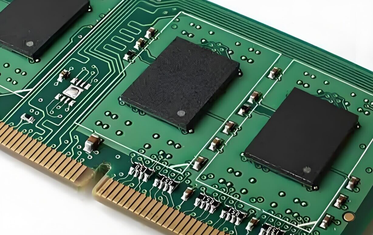
Thermal Pads
For heat generating components such as power transistors or voltage regulators, thermal pads help dissipate heat effectively by providing a direct thermal connection to the PCB ground plane or a specified heat sink. Thermal pads are specialized components used in electronics and thermal management applications to facilitate efficient heat transfer between electronic components and heat sinks or other cooling solutions. These pads are designed to fill the gap between heat generating components, such as semiconductor devices, and heat sinks or heat spreaders. Their primary goal is to improve thermal conduction, ensuring that excess heat generated by the component is effectively dissipated, thereby preventing overheating and maintaining optimal operating conditions. Thermal pads are used in a variety of electronic devices and industries.

Thermal Pads
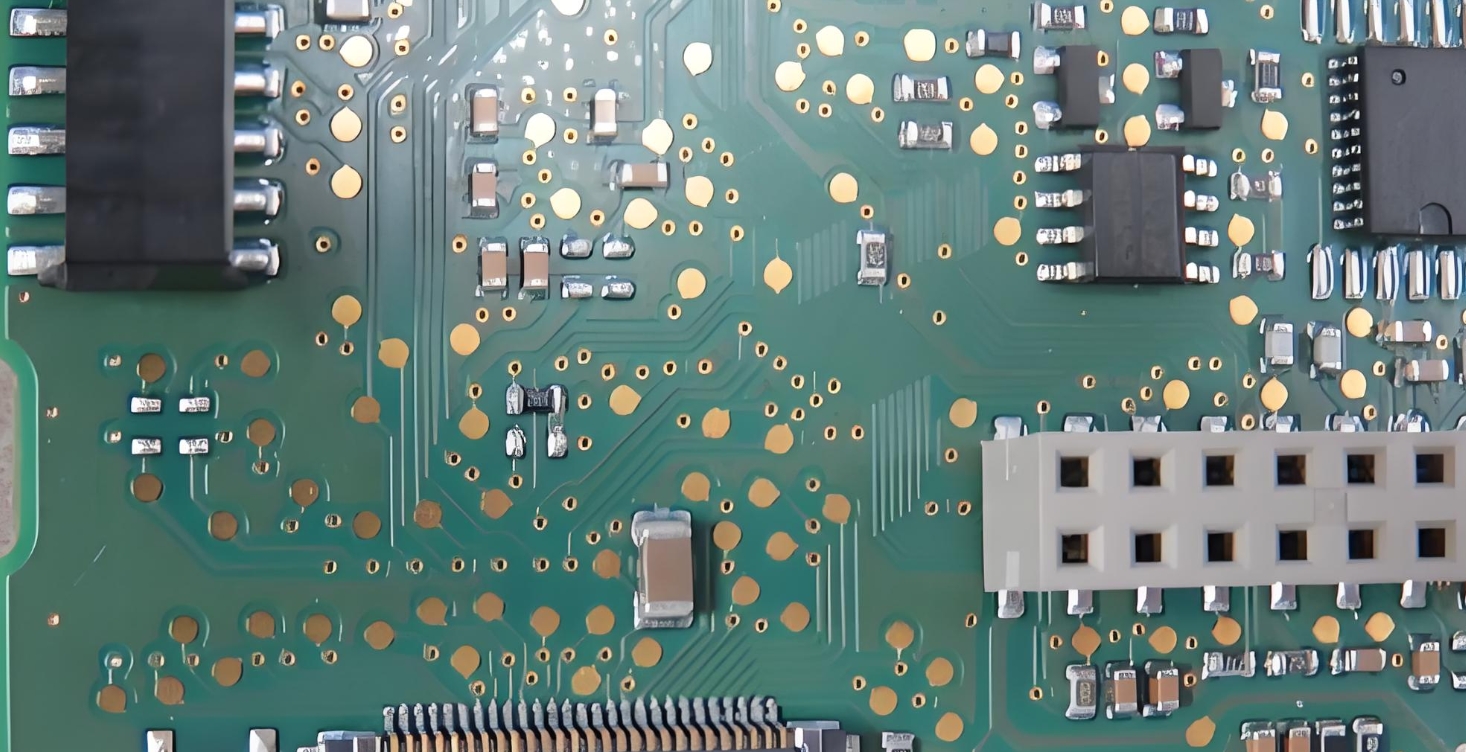
Test Pads
In the context of electronics and Printed circuit boards (PCBs), test pads are designated areas on a PCB that are specifically designed for testing and diagnostics during various stages of the manufacturing process and throughout the lifecycle of an electronic device. These pads serve as access points for probing, measuring, and verifying the functionality of components and circuits on the PCB.

Test Pads
Importance of PCB Pads
PCB pads are essential for connecting components to circuit boards, ensuring the flow of signals and power. Their design influences solder joint reliability and heat transfer, contributing to the performance and durability of electronic devices. As technology advances, the need for precise pads grows, enabling miniaturization and complex designs. They also facilitate quality control and testing, ensuring devices meet performance standards. Ultimately, PCB pads are critical to modern electronics, supporting innovation and functionality in a variety of applications.
Printed circuit board (PCB) pads are essential yet often overlooked components that facilitate the functionality and reliability of modern electronics. These small conductive areas connect various electronic elements, playing a crucial role in signal transmission and power distribution. Their precise design is vital for ensuring device quality and performance. As technology advances, PCB pads will continue to drive innovation, enabling the development of compact and efficient devices that power communication networks, medical advancements, and space exploration, showcasing their importance in engineering excellence.