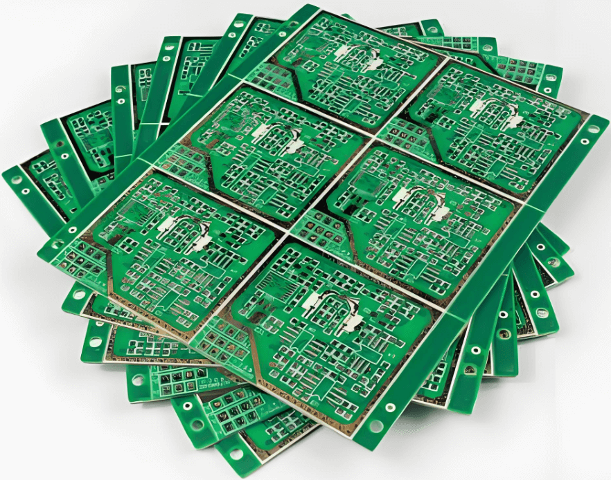
Overview of Multi-Layer Printed Circuit Boards
Multi-layer printed circuit boards (PCBs) consist of two or more conductive layers, typically copper, stacked and bonded together using a resin layer (prepreg). A crucial part of the manufacturing process includes drilling and electroplating to create predefined interconnections between the layers. This innovative technique deviated from traditional manufacturing processes by integrating multiple circuit layers, enabling the design of complex, high-density interconnections.
The inner layers of a multi-layer PCB are often based on double-sided constructions. This dual-layer foundation is subjected to various processes: the layers are drilled, electroplated, pattern transferred, developed, and etched before being laminated onto independent single-sided panels. The outer layers serve as signal layers that are plated through to create robust connections. The interaction between these layers allows for efficient component interconnection through wave soldering.
The complexity that comes with multilayer PCBs correlates with their manufacturing costs. These boards are generally regarded as the most sophisticated type of PCBs, presenting challenges in throughput and reworking compared to simpler designs.

Multi-layer PCB
Design Considerations
The proliferation of integrated circuit packaging has led to a high demand for interconnection lines, prompting the need for multilayer designs. As circuit designs evolve, challenges such as noise, stray capacitance, and crosstalk must be addressed. Effective PCB design strategies focus on minimizing signal line lengths and avoiding parallel routing, which can complicate layouts. For configurations with extensive interconnection requirements, multilayer boards provide the necessary routing flexibility that simpler designs (like single- or double-sided boards) cannot achieve.
Typically, a multilayer PCB features two outer conductive layers and a minimum of one additional conductive layer embedded within an insulating substrate. Electrical connectivity across layers is generally accomplished through plated through-holes. Absent specific instructions, multilayer boards usually include plated-through holes, akin to double-sided boards.
Current Trends in PCB Assembly
In the surface mount technology (SMT) industry, the predominant assembly method for circuit boards is full board reflow soldering. This can be categorized into single-sided and double-sided reflow techniques, with double-sided reflow being the more widely adopted due to its efficiency in space-saving and production volume, resulting in a preference for double-sided reflow processes in the market.
Characteristics of Double-Sided Circuit Boards
The defining distinction between single-sided and double-sided circuit boards lies in the number of copper layers. Double-sided boards feature copper layers on both sides, allowing for interconnections through vias. In contrast, single-sided boards have copper on only one side and are limited to simpler circuit designs with only plug-in connections.
As the demand for greater wiring density increases, technical considerations such as reducing hole diameters become essential. The reliability of double-sided boards hinges on the quality of the metallized holes which provide layer-to-layer connectivity. As hole sizes decrease, remaining debris—such as dust or residue—can negatively impact the electroplating process, leading to insufficient copper coverage and potentially compromising the integrity of the circuit.
Both sides of double-sided boards contain wiring, necessitating efficient circuit connections via what are known as vias. Vias are small, metal-coated holes that allow for electrical connections between the two sides of the PCB. The increased surface area and the ability to interleave wiring make double-sided boards suitable for more complex circuit designs compared to their single-sided counterparts.
In summary, double-sided printed circuit boards offer advanced design possibilities and flexibility for complex electronic applications, enabling higher wiring densities and improved functionality essential in modern electronics.