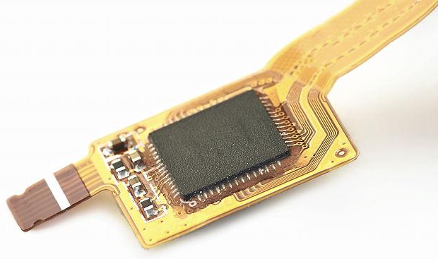
In the ever-evolving landscape of electronics, the demand for smaller, lighter, and more efficient products continues to grow. One significant advancement that has risen to meet these demands is the High-Density Interconnect Flexible Printed Circuit Board. This technology is crucial in various industries, including consumer electronics, automotive, aerospace, telecommunications, and medical devices. In this blog, we will explore the characteristics, manufacturing processes, applications, and technical specifications of HDI Flex PCBs in detail.

HDI Flex PCB
What is an HDI Flex PCB?
High-Density Interconnect Flexible PCBs are advanced circuit boards characterized by their high wiring density and the use of flexible substrates. HDI technology enables the integration of more components onto a smaller surface area, facilitating complex circuit designs. The flexibility of HDI boards allows them to conform to various shapes and fit into compact spaces, making them ideal for modern electronic applications.
Key Characteristics of HDI Flex PCBs
High Wiring Density: HDI PCBs utilize finer traces and spaces along with microvias, which allow for a greater number of connections in a smaller area. This is especially valuable in devices with limited space.
Flexible Substrates: These PCBs are made from materials like polyimide or polyester, which offer excellent flexibility and durability. This adaptability allows them to bend and flex without risking damage to the circuitry.
Multilayer Configuration: HDI Flex PCBs can have multiple layers that enhance functionality. These layers can include routing for both surface-mount and through-hole components, offering greater design versatility.
Microvia Technology: Microvias are small-diameter holes that connect different layers of the PCB. They provide routing pathways that result in smoother designs with less wiring clutter.
Lightweight and Compact: High-density designs reduce the overall weight and size of electronic devices, making HDI Flex PCBs particularly attractive for portable applications.
Heat Resistance: Materials used in HDI Flex PCBs can withstand high temperatures, making them suitable for applications requiring thermal stability.
Technical Specifications of HDI Flex PCBs
Layer Stack-up
The layer stack-up of HDI Flex PCBs can vary widely depending on the design requirements and the number of components. Typically, HDI Flex PCBs can carry anywhere from 1 to 20 layers or more, with common stack-ups found in 4-layer, 6-layer, and 8-layer configurations. The flexibility of the design allows for diverse stack-ups, including:
Layer Configuration: An HDI Flex PCB typically consists of 2 to 20 layers, though more layers can be utilized depending on the complexity of the design. Each layer is utilized for specific functions, such as power distribution, signal routing, or ground connections.
Types of Layers:
Signal Layers: These are responsible for transmitting electrical signals and can be placed on the outer or inner layers.
Ground and Power Layers: Dedicated layers are used for ground and power planes to reduce electromagnetic interference (EMI) and improve signal integrity.
Dielectric Layers: These insulating layers separate conductive layers, providing the necessary separation while allowing for flexible movement.
Microvia Implementation: HDI designs heavily rely on microvias to connect layers. These microvias can be blind (connecting only one outer layer to an inner layer) or buried (connecting inner layers without going to the outer layer), allowing for efficient use of space and improved performance.
Copper Thickness: The thickness of the copper in the conductive layers is an important consideration. HDI Flex PCBs typically use thinner copper (1-1.5 oz) for better performance and thermal management. However, thicker copper can be used for power delivery applications that require higher current handling.
Stack-up Variations: Depending on the specific application and design requirements, various stack-up configurations can be employed. Some common configurations include:
4-Layer Stack: Often used for simpler applications where there are distinct power and ground onnections.
6-Layer Stack: Provides a balance between complexity and space efficiency, suitable for mid-range designs with multiple signal layers.
8-Layer and Beyond: Used in high-performance designs requiring significant routing capabilities, advanced EMI shielding, and complex interconnections.
Impedance Control: Maintaining controlled impedance is essential for high-speed applications. Designing the stack-up with specific dielectric thicknesses and copper widths ensures consistent impedance across the traces, minimizing signal degradation.
Applications of HDI Flex PCBs
The versatility and advantages of HDI Flex PCBs make them suitable for various applications across multiple industries:
Consumer Electronics: From smartphones and tablets to gaming consoles, HDI Flex PCBs are integral to the compact design and high functionality of consumer devices.
Medical Devices: In the medical field, many handheld diagnostic tools and wearable health monitors use HDI Flex PCBs due to their lightweight nature and capability of integrating multiple sensors.
Automotive Industry: Vehicles are becoming increasingly sophisticated, incorporating advanced driver-assistance systems (ADAS) and infotainment systems that rely on HDI Flex PCBs for their compact electronic assemblies.
Aerospace and Defense: In avionics and military applications, HDI Flex PCBs are essential for ensuring reliability in adverse conditions while maintaining a lightweight profile.
Telecommunications: The infrastructure supporting telecommunications, such as base stations and antennas, utilizes HDI Flex PCBs for efficient signal processing and connectivity.
Robotics and Industrial Automation: HDI Flex PCBs are leveraged in robotic systems and automation equipment, where space efficiency and flexibility in design are vital.
Conclusion
High-Density Interconnect Flexible PCBs represent a pinnacle of modern electronics design, combining high-density interconnections with flexibility and lightweight materials. Their ability to facilitate compact, efficient designs has made them indispensable in contemporary consumer electronics, medical devices, automotive systems, and beyond. The various stack-up options and microvia technologies enable engineers to create complex multilayer configurations that accommodate the growing demands for functionality and performance in electronic devices.
As technology continues to advance, the role of HDI Flex PCBs will undoubtedly expand, driving innovation and enhancing the capabilities of electronic devices. Understanding this technology is essential for engineers, manufacturers, and developers aiming to stay at the forefront of electronic design.