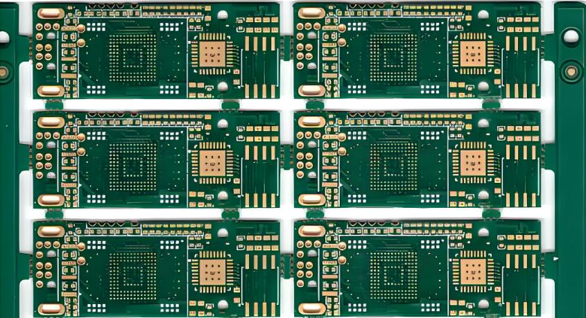
High-Density Interconnect (HDI) printed circuit boards represent a cutting-edge technology designed to maximize functionality within the same or even smaller physical dimensions of traditional PCBs. This advancement has enabled significant innovations across various sectors, particularly in consumer electronics such as smart phones and laptops. Additionally, HDI technology plays a crucial role in specialized applications including touch-screen devices, 4G-5G communications, and military technologies like avionics and advanced military systems.

HDI PCB
Key Characteristics of HDI PCBs
HDI PCBs are defined by their unique characteristics:
Increased Wiring Density: Incorporating features such as laser-drilled micro vias, fine traces, and high-performance dielectric materials, HDI PCBs support a higher density of electrical pathways.
Multi-layer Stack Technology: These boards utilize multiple layers of stacked copper-filled microvias, facilitating complex interconnections necessary to accommodate the high pin counts prevalent in modern electronics.
For instance, while designing high-tech devices, engineers often rely on the intricate routing capabilities of High-Density Interconnect (HDI) Printed Circuit Boards to manage connections for powerful CPUs and GPUs.
HDI Architecture Basics
The architecture of HDI PCBs is often described by specific layer configurations:
1 + N + 1: This setup includes one standard layer combined with a high-density interconnect layer.
I + N + I (where I ≥ 2): This structure entails multiple layers featuring high-density interconnects, where the microvias can be staggered or stacked to enhance functionality. This arrangement is particularly effective in complex PCB designs that require advanced connectivity.
Comprehensive HDI Board: In this design, every layer consists of high-density interconnects, allowing for flexible connections across all layers via multi-layered, stacked copper-filled microvias. This configuration is ideal for connecting large pin-count components, such as those found in modern handheld devices.
Advanced Micro holes in HDI PCBs
The advanced micro holes, produced through laser drilling, typically range from 0.004 inches (100 μm) to 0.006 inches (150 μm) in diameter. These micro holes are precisely aligned with corresponding pad diameters (e.g., 0.008 inches or larger), which enhances the overall wiring density.
Options for micro hole design include:
Directly Aligned Pad Design: Micro holes can be designed directly on the pads or can deviate slightly, enabling flexibility in layout.
Staggered or Stacked Configurations: This approach enhances connectivity and supports the sophisticated wiring requirements of fine-pitch BGAs (Ball Grid Arrays), particularly those less than 0.8 mm.
For even finer pitches, such as 0.5 mm, interleaved micro holes are utilized, while micro-BGA applications (0.4 mm, 0.3 mm, 0.25 mm pitches) necessitate stacked micro holes implemented through advanced wiring techniques like inverted pyramid designs.
Experience and Innovation at IPCB
At IPCB, we leverage years of experience in producing HDI PCB products, standing at the forefront of the second generation of micro via technology. Our advanced stacked micro pore solutions offer robust and flexible wiring configurations for even the most demanding micro BGA applications. By continually adapting to technological advancements, we ensure that we meet the evolving needs of our clients in various industries.