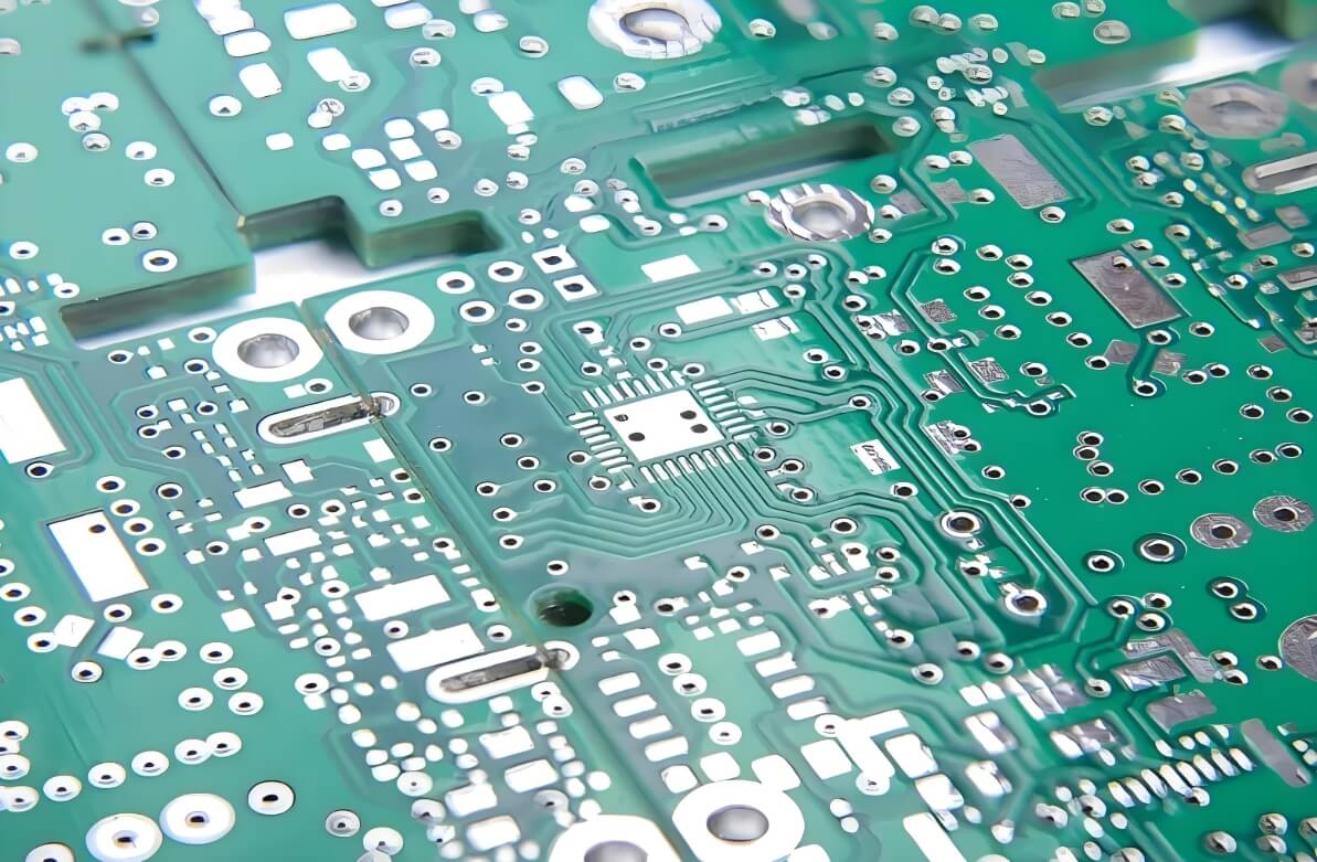
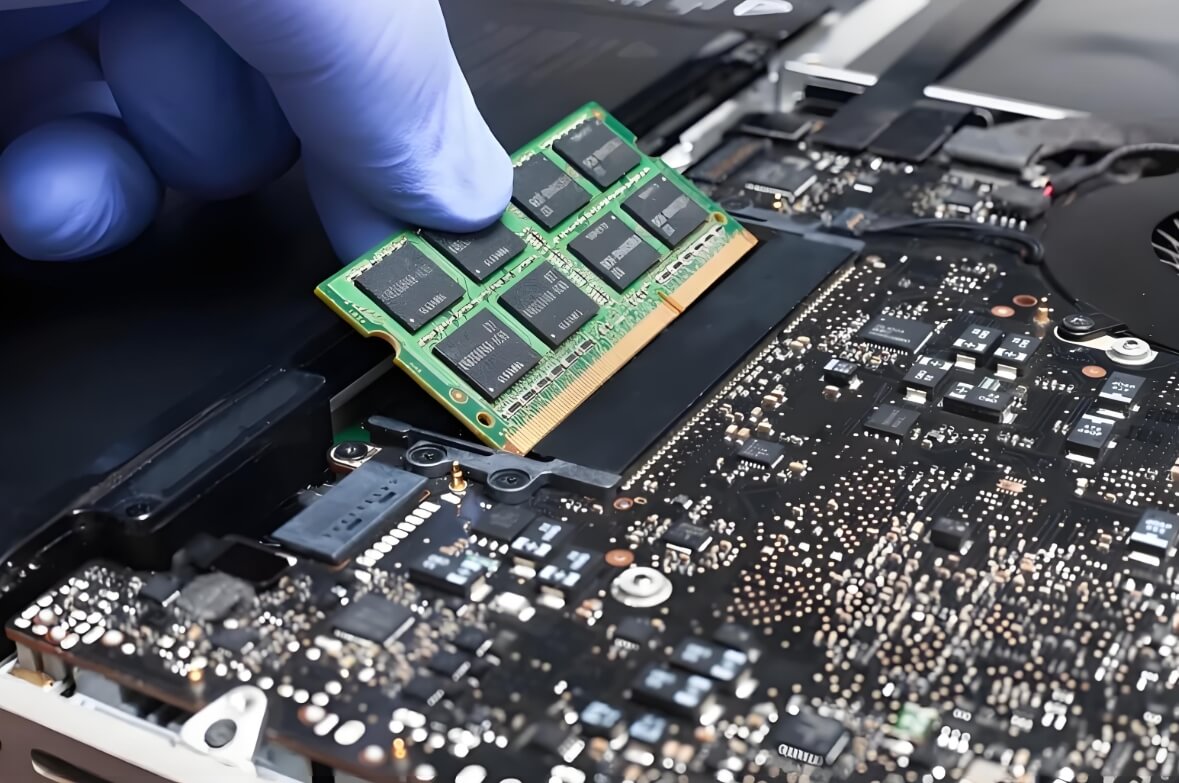
A Multilayer PCB is a printed circuit board with more than two layers, typically containing at least three conductive copper layers. While the top and bottom layers resemble a double-sided PCB, additional inner layers are used for routing, with interconnections made through copper-plated holes. Multilayer PCBs can have up to 40 layers, with common applications ranging from 4-8 layers in smart devices to 12 layers in smartphones.
Manufacturers prefer an even number of layers to reduce complexity and costs. In a 4-layer PCB, signal layers are placed near power and ground planes to enhance electromagnetic compatibility (EMI) and minimize noise. Higher-layer count PCBs use thin dielectric materials for better signal integrity and EMI performance, often used in high-speed electronics. More layers increase the board's thickness.
How Multilayer PCBs Work:
The manufacturing process of multilayer PCBs starts with designing the board layout using PCB design software. Once the design is complete, the inner layer core is created and laminated with copper foil, dry film resist, and UV light. The lamination process stacks the core, prepreg sheets, and copper foil, which is then subjected to heat, pressure, and vacuum to bond the layers together.
The design typically dedicates one layer to the ground plane and another to the power plane, with the remaining space used for signal tracks. In a six-layer PCB, there are four signal layers and two power layers. Multilayer PCBs feature two reference planes and signal vias for electrical flow, with stitching vias to optimize signal routing. Different types of vias—standard, blind, and buried—are used to enhance routing density.
What is a PCB Via?
A via is an electrical connection between different layers of a PCB, appearing as a small hole coated with copper to create a conductive path. Vias are designed to connect layers in a PCB and are different from larger plated through holes used for through-hole components. There are three types of vias:
Standard (Through-Hole) Via: Passes through all layers, connecting the top, bottom, and inner layers. These are larger and simpler to manufacture.
Blind Via: Connects outer layers to inner layers but doesn't pass through the entire board. It is used to improve connections between layers but requires precise drilling.
Buried Via: Connects only inner layers and is not visible from the outer layers. These reduce board size but can increase manufacturing costs due to the need for precision in design and production.

PCB Vias
Advantages of Multilayer PCBs:
Reduced Form Factor: Multilayer PCBs allow for smaller, more compact designs without sacrificing functionality. This makes them ideal for devices like smartphones and wearables, where space is limited.
Lightweight Boards: Advanced manufacturing techniques reduce the weight of multilayer PCBs, making them suitable for lightweight applications such as smart devices. The use of fewer connectors between layers also contributes to the reduction in weight.
Multifunctionality with High Quality: Multilayer PCBs can integrate multiple functions into a single board, offering capabilities that single-layer boards can't achieve. This is especially beneficial in devices like smartphones, where diverse features are packed into a small footprint.
Durability and Flexibility: Multilayer PCBs are built to withstand mechanical stress, heat, and pressure, ensuring durability for long-term use. They also offer flexibility, allowing for modifications without needing a complete redesign.
Single Connection Point: Unlike multiple single-layer PCBs, multilayer PCBs offer a single connection point, simplifying the design and reducing complexity in the overall system.
Disadvantages of Multilayer PCBs:
Elevated Cost of Production: Multilayer PCBs are more expensive to produce than single or double-sided PCBs. The manufacturing process involves more labor, advanced design, and costly assembly machinery, contributing to the higher cost.
Complex Design Process: Designing multilayer PCBs is time-consuming and requires careful adherence to many design rules. The selection of lamination and substrate materials also depends on the specific application and the components used, which adds to the complexity.
Required Domain Expertise: Multilayer PCBs require specialized knowledge and experience in using CAD tools and performing design rule checks. Due to the challenges in the design and manufacturing process, domain expertise is essential to ensure the board meets all requirements and performs as expected.
Multilayer PCB Applications:

PCB Application
Consumer Electronics: Essential for smartphones and smart devices due to their small size, multifunctionality, and compact design.
Telecommunication Industry: Used in network appliances and transmission devices for their flexibility and durability in both outdoor and indoor environments.
Manufacturing Industry: Withstands extreme pressure, heat, and high temperatures, making them ideal for industrial setups and production lines.
Medical Devices: Lightweight and robust, ensuring precise and reliable performance in medical equipment for diagnosis and treatment.
Military and Defense: Offers durability, compact design, and lightweight features, providing more room for components and custom functionalities.
Automotive and Aerospace: Withstands extreme conditions while maintaining precision and functionality, ensuring high-quality performance in these demanding sectors.
Multilayer PCBs play a crucial role in modern electronic devices, offering a compact, durable, and multifunctional solution for various industries. From consumer electronics and telecommunications to aerospace and defense, their ability to withstand extreme conditions while maintaining high performance makes them indispensable in advanced applications. As technology continues to evolve, the demand for multilayer PCBs will only grow, supporting the development of smaller, more efficient, and reliable electronic systems.