Share cost-effective products and high-quality services with customers. Contact Us


In the dazzling realm of microelectronics, where chips shrink to unimaginable sizes and performance demands skyrocket, there's an often-overlooked yet absolutely vital component: the IC substrate PCB. While the main printed circuit board assembly gets much of the spotlight, the intricate dance happening within and around the integrated circuit package is largely orchestrated by this unsung hero. For over fifteen years, we've witnessed firsthand the evolution of IC substrate technology, from simpler interconnect solutions to the sophisticated, high-density powerhouses we see today. In this blog post, we'll peel back the layers of these critical components, exploring their purpose, construction, key considerations, and the exciting future they hold.

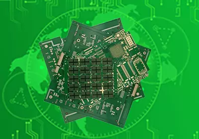
IC Substrate PCBs
Bridging the Gap: Why IC Substrates Matter
Think of an integrated circuit as a highly complex city packed onto a tiny silicon chip. This "city" needs robust infrastructure to connect its various districts (functional blocks) internally and, crucially, to the outside world. This is where the IC substrate PCB steps in. Its primary roles are:
Redistribution: The incredibly fine pitch of the connections on the silicon die needs to be fanned out to a more manageable pitch for connection to the main PCB. The substrate acts as an intermediary, redistributing these signals.
Interconnection: It provides the electrical pathways to connect the die to the external pins or balls of the IC package. This involves intricate routing of signal, power, and ground layers.
Power and Ground Distribution: With increasing chip power consumption and sensitivity to noise, the substrate plays a critical role in delivering clean and stable power and providing a low-impedance ground path.
Signal Integrity: As signal speeds climb, the substrate's material properties and design become paramount in maintaining signal integrity, minimizing reflections, and controlling impedance.
Thermal Management: Dissipating heat generated by the high-power IC is crucial for reliability. The substrate often incorporates thermal vias and materials with high thermal conductivity to channel heat away from the die.
Mechanical Support and Protection: The delicate silicon die needs a robust mechanical foundation and protection from physical stress and environmental factors. The substrate provides this structural support.
Peeling Back the Layers: Construction and Materials
IC substrates are multi-layered structures built using advanced PCB fabrication techniques. While the specific construction varies depending on the application, some common elements include:
Dielectric Layers: These insulating layers separate the conductive layers and are typically made of materials with excellent electrical properties, such as epoxy resins, polyimides, or more advanced materials like ABF (Ajinomoto Build-up Film). The choice of dielectric material significantly impacts signal integrity and thermal performance.
Conductive Layers: These layers, usually made of copper, are patterned to create the intricate signal traces, power planes, and ground planes. The thickness and patterning of these layers are critical for current carrying capacity and impedance control.
Vias: These are conductive pathways that connect different layers. Various types of vias are used, including through-hole vias, blind vias (connecting an outer layer to one or more inner layers), and buried vias (connecting only inner layers). Microvias, with their extremely small diameters, are essential for high-density substrates.
Solder Mask and Surface Finish: Similar to traditional PCBs, a solder mask protects the outer layers and prevents shorts during assembly. Surface finishes like ENIG (Electroless Nickel Immersion Gold) provide a reliable and corrosion-resistant surface for bonding.
The materials used in IC substrates are carefully selected based on a multitude of factors, including:
Electrical Performance: Dielectric constant (Dk) and loss tangent (Df) are critical for high-speed signal transmission.
Thermal Performance: Thermal conductivity and coefficient of thermal expansion (CTE) are important for managing heat and ensuring reliability under temperature variations.
Mechanical Properties: Flexural strength and adhesion between layers are crucial for withstanding assembly and operational stresses.
Reliability: Materials must be able to withstand harsh environmental conditions and long-term operation.
Cost: Material costs can significantly impact the overall cost of the IC package.
Key Considerations in IC Substrate Design
Designing an effective IC substrate is a complex undertaking that requires a deep understanding of electrical, thermal, and mechanical principles. Here are some key considerations:
Signal Integrity: With increasing data rates, meticulous attention must be paid to impedance matching, crosstalk minimization, and signal reflection control. Advanced simulation tools are essential for analyzing and optimizing signal paths.
Power Integrity: Ensuring clean and stable power delivery to the die is paramount. This involves careful placement of decoupling capacitors, minimizing inductance in power distribution networks, and managing simultaneous switching noise.
Thermal Management: As IC power densities rise, effective heat dissipation becomes increasingly challenging. Substrate design must incorporate thermal vias, heat spreaders, and consider the thermal interface materials used in the final assembly.
Design for Manufacturability (DFM): The intricate features of IC substrates require tight manufacturing tolerances. Design rules must be carefully followed to ensure high yields and reliable fabrication.
Cost Optimization: Balancing performance requirements with cost constraints is always a key consideration. Material selection, layer count, and feature sizes all impact the final cost.
Package Type: The choice of IC package (e.g., BGA, QFN) significantly influences the substrate design and the routing strategies employed.
The Future of IC Substraets: Trends and Innovations
The field of IC substrate technology is constantly evolving to meet the ever-increasing demands of the semiconductor industry. Some exciting trends and innovations include:
Higher Density Interconnect (HDI): Continued miniaturization of features, including finer lines and spaces, smaller vias, and tighter pitches, allows for more complex routing within a smaller footprint.
Advanced Materials: Research into new dielectric materials with lower loss and higher thermal conductivity is ongoing. Novel materials like glass substrates are also being explored for their superior electrical and mechanical properties.
3D Integration: Techniques like through-silicon vias (TSVs) and chiplets are driving the need for advanced substrates that can support vertical stacking and complex interconnections between multiple dies.
Embedded Components: Integrating passive components like resistors and capacitors directly into the substrate can save space and improve electrical performance.
Advanced Simulation and Analysis: Sophisticated simulation tools are becoming increasingly crucial for predicting and optimizing the electrical, thermal, and mechanical behavior of complex substrates.
Conclusion: The Foundation of Innovation
The IC substrate PCB, while often hidden from view, forms the critical foundation upon which modern microelectronics is built. Its intricate design and advanced materials enable the high performance, small form factors, and increasing functionality of today's electronic devices.
As we continue to push the boundaries of semiconductor technology, the role of the IC substrate will only become more critical. It's a testament to the ingenuity of engineers and material scientists who constantly innovate to meet the ever-growing demands of our increasingly digital world.