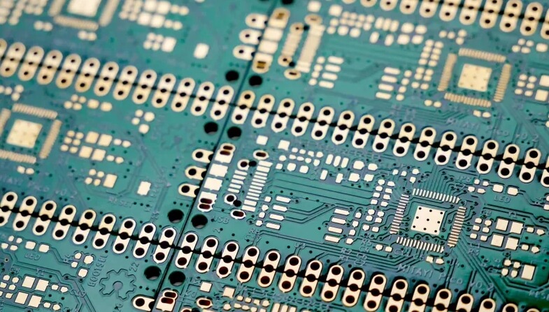
Vertical interconnect ports (or vias) are small electrical connections that allow electrical signals to be transmitted between different layers of a printed circuit board (PCB). If we think of traces as existing on the x- and y-axes of the board, vias exist on the z-axis. Structurally, they are like small vertical tubes coated with a layer of conductive material, such as copper or gold, and placed in a drilled hole. They are also filled with different substances to guarantee good conductivity and mechanical resistance.
Traditionally, if a pin needs to be connected to a via, a trace is created to route the signal away from its terminal. However, this approach is less efficient for densely packed surface mount technology (SMT) PCBs and certain integrated circuit (IC) packages, such as quad flat no-leads (QFN) and ball grid arrays (BGA).
What are the different types of vias?
Vias can be divided into a number of different variations depending on the type of connection being made. Let's look at some of the most commonly used.
Through-Hole Via
Through-hole vias are designed to connect all layers of a PCB at a specific point. These vias are created by drilling a hole through the board and plating it with copper (or other conductive materials) to establish a continuous electrical connection from the top layer to the bottom layer.
Through-hole vias are the most widely used type of via in PCB manufacturing due to their straightforward design and ease of production. They are also the most cost-effective and simplest to fabricate.
With advancements in precision manufacturing, more complex vias have been developed, enabling designers to bypass specific layers in multilayer PCBs. Examples of these specialized vias include blind vias, buried vias, microvias, and vias-in-pad.
Blind Via
Blind vias connect the outer layers of a PCB to one or more inner layers without passing through the entire board. They are visible from one side of the PCB but not the other, giving them their name.
Compared to through-hole vias, blind vias are more complex to manufacture and generally more expensive.
Buried Via
Buried vias are used to connect two or more internal layers of a PCB without extending to the outer layers, making them invisible from the surface. These vias are typically used in multilayer PCBs with four or more layers and are more challenging to manufacture compared to blind vias.
Microvia
Microvias are smaller, more compact versions of traditional vias, with a distinct structural difference. Unlike the cylindrical shape of standard vias, microvias are designed with a frustum-like structure, where the radius decreases as the via transitions between layers.
Due to reliability concerns, microvias are typically limited to connecting no more than two layers. For multi-layer connections, microvias are stacked vertically. Buried microvias are often filled with copper or conductive epoxy to enhance their strength and resistance to mechanical stress and pressure.

Via-in-pad Design
What is a Via in Pad?
A via in pad is a type of via that is positioned directly within the pad of an electronic component on the surface of a PCB. It creates an electrical connection between the outer layer and the internal layers of the PCB. Vias in pad are commonly used in applications such as High-Density Interconnect (HDI) PCBs and high-frequency boards, particularly where integrated circuits (ICs) with Ball Grid Array (BGA) packages are used. These vias are essential for routing signals in dense and complex PCB designs.
Via-in-Pad Applications
Vias-in-pads are used in PCB designs when space is limited, especially in BGAs (Ball Grid Arrays), where pin density is high. BGAs offer higher packing efficiency but make surface routing difficult due to tiny solder balls and tight pin spacing. Instead of routing traces far from the component, vias can be placed directly under the BGA pads to connect the signals to the required PCB layers, simplifying the design and avoiding track clearance issues.
Advantages of Via-in-Pad Routing
Space Efficiency:
Vias-in-pads save space by placing the via directly under the component pad, reducing the need for additional routing tracks and shrinking the PCB footprint.
Simplified Routing:
Directly placing vias under pads simplifies routing, especially for small components like BGAs.
Improved Heat Dissipation:
Vias near heat-sensitive components enhance thermal conductivity, allowing faster heat dissipation.
Reduced Parasitic Inductance:
Vias in pads minimize parasitic inductance, improving signal integrity and enabling better placement of bypass capacitors in high-speed designs.
Drawbacks of Via-in-Pad Technology
While via-in-pad offers advantages, it comes with some challenges:
Higher Costs:
Creating vias in pads requires extra materials (conductive epoxy) and steps in the manufacturing process, increasing costs. These expenses don’t decrease proportionally with larger production volumes.
Surface Irregularities:
Improper placement or filling of vias can lead to surface bumps, complicating soldering, especially for small components.
Increased Design Complexity:
Designing via-in-pad layouts is more complex and requires careful planning for proper functionality.
Conventional Vias vs. Vias-in-Pad in PCB Design
Though vias-in-pad serve the same function as traditional vias, there are key design considerations:
Verify Manufacturer Capabilities:
Check the PCB manufacturer's specs, such as minimum annular ring size, to avoid DRC and DFM issues.
Export and Review Files:
Ensure you provide separate files for vias-in-pad and drill maps to prevent traditional vias from being capped.
Via Capping:
Vias-in-pad require capping during fabrication to prevent solder wicking, though leaving vias uncovered under thermal pads can improve heat dissipation.
Vias are essential for transferring electrical signals between the layers of multi-layer PCBs. Instead of routing a signal away from a pin and using a traditional via, vias can be placed directly on pads. This approach saves space, simplifies routing, enhances thermal management, and reduces parasitic inductance. However, vias in pads tend to be more expensive than conventional vias. Designers must confirm their PCB manufacturer's design capabilities and ensure that all necessary files are extracted from the design tool to guarantee smooth manufacturing.