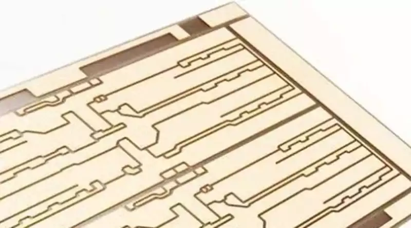
Product Name:Ceramic PCB
Material:CEM-3,Ceramic
Thickness: 10-25um
Copper thickness: 1OZ
Surface technology: ENIG/OSP/HSAL
Solder mask: White/Black/
Silk screen: White
Minimum line width/spacing: 0.075mm/0.15mm
Minimum through-hole: 0.1mm
Application:LED
A ceramic pcb is a PCB board made from a substrate or base plate of ceramic material, usually an inorganic dielectric, rather than a conventional glass fibre or epoxy resin substrate. It is an electronic circuit board made of a thin insulating layer of ceramic material with a metallic component.
Ceramic pcb characteristics:
High thermal conductivity:With different preparation processes and material combinations, ceramic substrates can reach a thermal conductivity of about 220 W/M.K, a value that far exceeds that of conventional FR-4 and CEM-3 circuit boards.
Outstanding electrical properties: Ceramic materials exhibit excellent high frequency and electrical properties, as well as excellent chemical and thermal stability.
Well-matched coefficients of thermal expansion: Ceramic circuit boards are much closer to the coefficients of thermal expansion of electronic assemblies, helping to alleviate stress problems caused by temperature changes.
Good solderability: ceramic pcb is easy to solder and can withstand high temperatures, making them suitable for use in electronic packaging under high-temperature conditions.
Excellent insulating properties: Ceramic materials have excellent insulating properties, ideal for high-voltage, high-frequency electronic applications.
Low High Frequency Loss: In high frequency circuits, ceramic pcb exhibits low loss, making them suitable for such applications.
High-density assembly capability: Because of its high density and strength, ceramic pcb supports the assembly needs of high-density electronic components.
Depending on the manufacturing process, ceramic PCBs can be classified into a variety of different types, the following are popular and frequently used on the market today:
Laser Activated Metallisation PCB (LAM PCB)
In the LAM process, the ceramic material is ionised and tightly bonded to the metal through the use of high-energy, high-intensity laser drilling. This process grows both together, creating a strong and deep connection. This connection then results in a superior and smoother surface texture. Currently, LAM and DPC technologies are becoming increasingly popular and widely used.
Direct Plated Copper PCB (DPC PCB)
This is a cutting-edge coating technology, a new ceramic substrate process that uses thin copper for line printing and etching, and plating it onto a ceramic substrate. Physical Vapour Deposition (PVD) technology, vacuum and sputtering innovations are used in the manufacture of DPCs to bond copper to the substrate under high temperature and pressure. Copper layer thicknesses for this process range from 10 microns (approximately 1/3 ounce) to 140 microns (4 ounces).
Direct Bonded Copper PCB (DBC PCB)
In the DBC process, an appropriate amount of oxygen is introduced between the copper and the ceramic before or during the deposition process. This method is used when high copper layer thicknesses of 140 microns (4 ounces) to 350 microns (10 ounces) need to be achieved.
Low Temperature Co-fired Ceramic PCB (LTCC PCB)
This type of PCB can be manufactured with or without the use of glass. Traditionally, a ceramic substance is mixed with 30 to 50 per cent glass material to create LTCC PCBs. an organic binder is added to the mixture to ensure that the materials bond properly. After the mixture is applied to the sheet and dried, through-holes are drilled according to the design layout of each layer. Screen printing technology is used to print the circuits and fill the holes. The baking process is done in an oven at a temperature range usually between 850 and 900 degrees Celsius. The traces created by this method are usually gold in colour.
High Temperature Co-fired Ceramic PCB (HTCC PCB)
HTCC PCBs are built from scratch using virgin ceramic substrate material. No glass material is ever added during the production process.The only difference between the HTCC and LTCC production processes is that HTCC PCBs are baked in a gaseous environment at temperatures of approximately 1600 to 1700 degrees Celsius. Due to the extremely high co-firing temperatures of HTCC PCBs, circuit alignments made of high melting point metals such as tungsten, molybdenum or manganese are used. At high temperatures, these PCBs can still function without damage because they are designed to be stable even in harsh environments.
Thick Film Ceramic PCB
These PCBs are ideal when oxidation is a factor to be considered. This is why, after coating the ceramic substrate with dielectrics, gold, silver, or copper for a wide range of applications, the material needs to be baked in a nitrogen atmosphere to 1000 degrees Celsius. Due to the effective protection against oxidation, capacitors, resistors, conductors and semiconductors on ceramic boards are interchangeable. The conductor layer can be 10 to 13 microns thick.

Several commonly used manufacturing processes for ceramic pcb:
1.Moulding Manufacturing Method:This process starts with mixing ceramic powder with an organic binder, which is subsequently pressed on a mould to form a board structure. This is followed by drying and sintering, and finally the desired circuit is formed by removing excess wires and components.
2.Flux Coating Manufacturing Method: In this method, the circuit pattern is first coated on the ceramic pcb with flux, and then the metal film required for soldering is uniformly coated with flux using techniques such as electrophoresis, spraying or screen printing.Finally,drying and sintering are carried out.
3.Die-casting moulding and component fixing manufacturing method:this process mixes ceramic powder with organic binder and presses it into a plate shape, and then uses a die-casting machine to accurately fix pre-fabricated wire components onto the ceramic substrate. Finally, it is dried and sintered.
4.Contactless Printing Manufacturing Method: This method uses advanced contactless printing technologies such as inkjet,light-curing or laser to print circuit patterns and metal wires directly on the ceramic pcb.
Product Name:Ceramic PCB
Material:CEM-3,Ceramic
Thickness: 10-25um
Copper thickness: 1OZ
Surface technology: ENIG/OSP/HSAL
Solder mask: White/Black/
Silk screen: White
Minimum line width/spacing: 0.075mm/0.15mm
Minimum through-hole: 0.1mm
Application:LED
iPCB Corporation provides support for PCB Prototype and Electronic Manufacturing. You can request consultation or quotation for PCB, PCBA and ODM here, please contact email: sales@ipcb.com
We will respond very quickly.