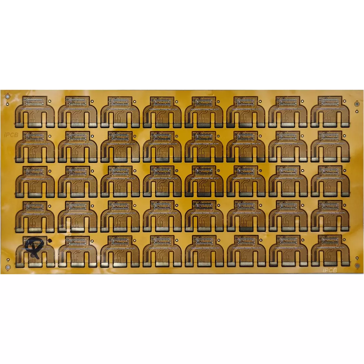
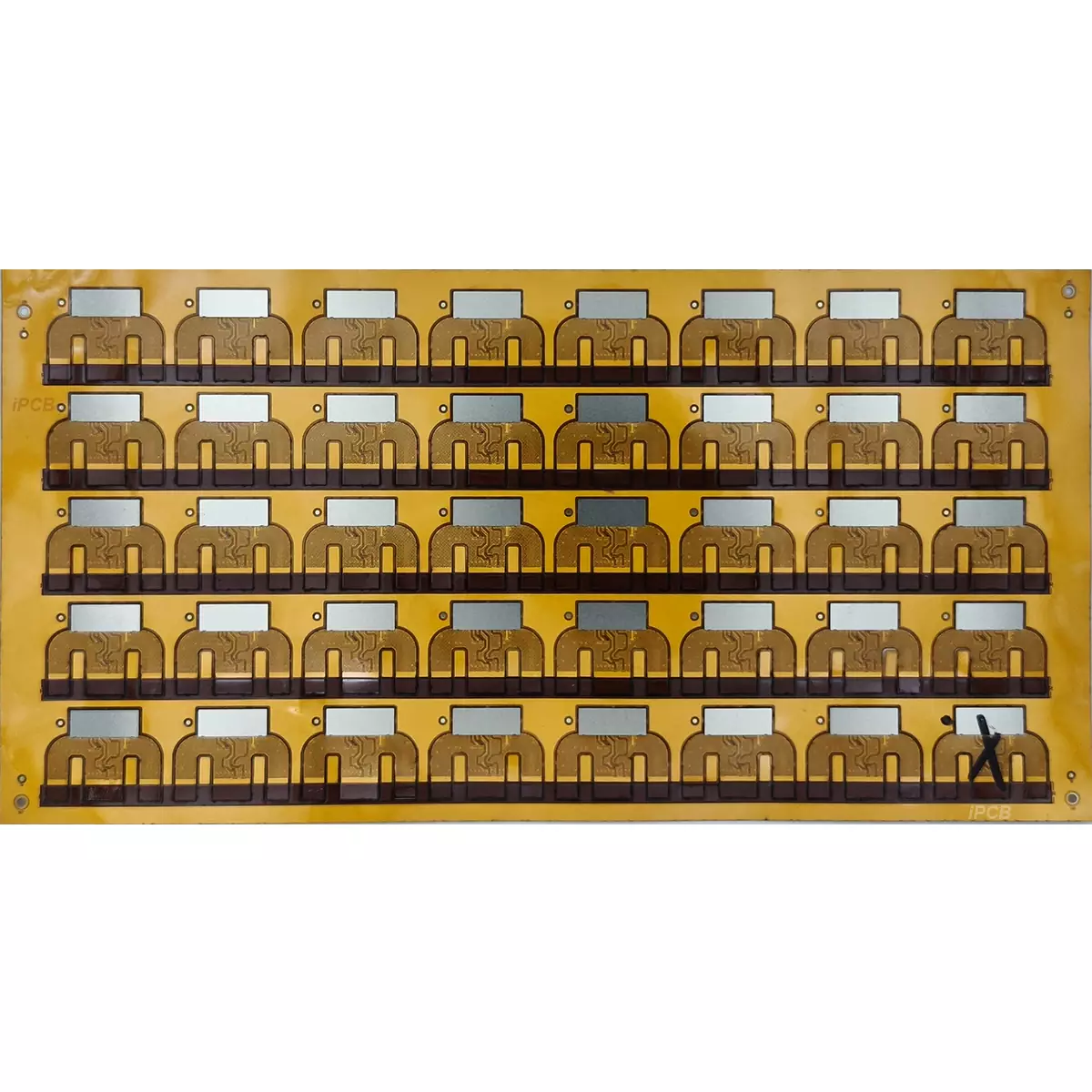
Product Name:Flexible pcb
Material:PI,PET
Thickness: 0.1mm+0.8mm
Copper thickness: 1/3OZ ~1OZ
Surface technology: Immersion gold
Solder mask: White/Green/Yellow
Silk screen: White
Minimum line width/spacing: 2mil
Minimum through-hole: 0.1mm
Application:Various electronic product
The fpc full form is Flexible Printed Circuit,which is called Flexible Printed Circuit Board,Flexible pcb in Chinese.As the name suggests,this circuit board is soft and bendable,unlike our common rigid PCB (Printed Circuit Board). It is a circuit board made of flexible substrate,usually using polyester film,polyimide (PI) or polyamide (PA) and other high-performance materials.Compared to traditional rigid boards,FPC is bendable and flexible, making it suitable for electronic devices and products that require curved or complex shapes.It is characterised by high wiring density, light weight,thin thickness and good bendability.
It originated in the early 20th century, when Paul Eisler, an American patent engineer, first proposed the concept of flexible circuits in 1936. By the 1970s,with the booming of the electronics industry, FPC was gradually widely used and evolved into higher technological forms.
Introduction of FPC basic structure materials
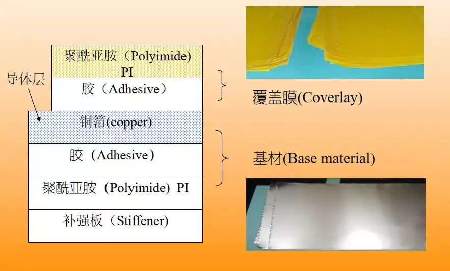
From the analysis of the basic structure of the flexible pcb,the composition of the flexible printed circuit board materials are insulating substrate, adhesive, metal conductor layer (copper foil) and cover layer.
(1) Copper foil substrate (Copper Film) copper foil: basically divided into electrolytic copper and calendered copper two. The common thicknesses are 1oz 1/2oz and 1/3oz. Substrate film: the common thicknesses are 1 mil and 1/2 mil. Adhesive: Thickness depends on your needs.
(2) Cover Film (Cover Film) Cover Film:For surface insulation.Common thicknesses are 1 mil and 1/2 mil. Adhesive: Thickness is determined by your needs. Release paper: to avoid adhesive in the pressure before the adhesive attached to foreign objects; easy to work.
(3) Reinforcement plate (PI STIffener Film) Reinforcement plate:reinforce the mechanical strength of the FPC, to facilitate the surface mounting operations. Common thickness of 3 mil to 9 mil. adhesive (adhesive): the thickness according to their own needs to decide. Release paper: to avoid the adhesive in the pressure before the adhesion of foreign objects, EMI: electromagnetic shielding film, to protect the circuit board circuit from the outside world (strong electromagnetic area or susceptible to interference areas) interference.In addition,FPC often have pads,gold fingers and other structures, generally to strengthen its processing, that is, the reverse side of these structures at the pressure of the appropriate size of the FR4 or PI is not strong, the thickness of the product according to the specific use of the environment to choose, and, sometimes, will also be used in the steel sheet. Reinforcement can only be in the flexible pcb surface layer.
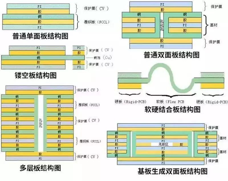
Based on the number of layers of conductors and structural differences, FPC can be divided into the following four common types:
Single-sided flexible pcb: These boards contain only one layer of conductors, the production process is relatively simple and low cost, often used in consumer electronics, smart home and other areas of the connection task.
Double-sided flexible pcb: This type of board has two layers of conductors, and if you need to establish an electrical connection between the two layers of conductors, you need to use the through-hole as a ‘bridge’. The through-hole is a small copper-plated hole in the wall that connects the conductors on both sides. Double-sided flexible pcb is a common type, widely used in digital cameras, handheld devices, LCDs, medical equipment and industrial control and many other fields.
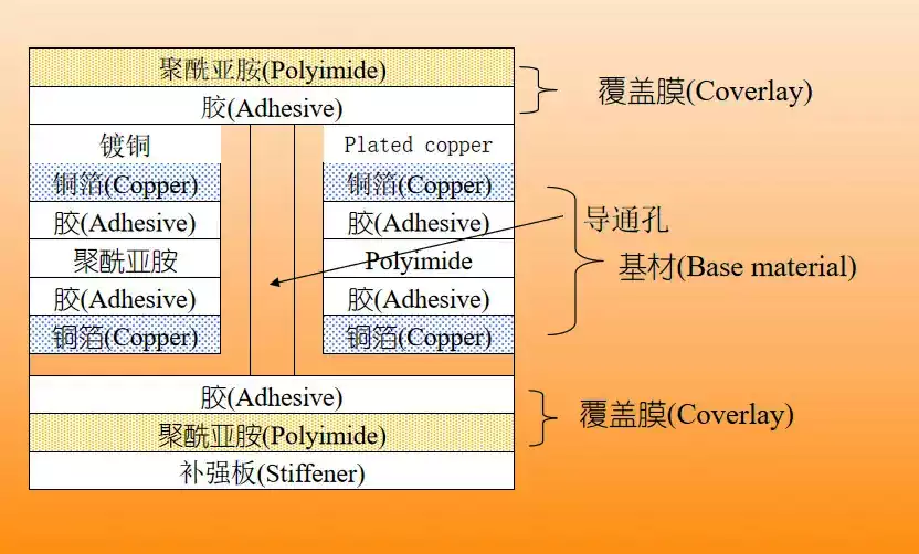
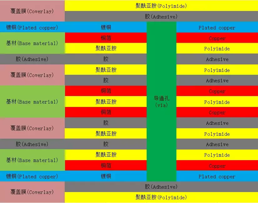
Multilayer flexible pcb: These boards have a complex structure, containing at least three layers of conductors, and the connection between the different layers needs to be realised through vias. The multi-layer conductor layer builds a high-density, high signal-to-noise ratio flexible circuit board structure, showing excellent anti-interference and anti-electromagnetic wave interference ability. It is commonly used for data transmission, signal processing, control, and power supply, and is used in high-end electronic products in mobile devices, medical devices, automobiles, smart homes, and other fields.
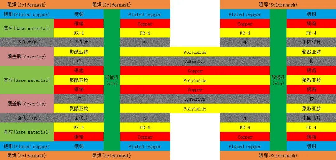
Rigid-Flexible Combination Board (R-FPC): This is a complex and costly board type that combines the advantages of rigid and flexible boards. Due to its excellent performance, Rigid-Flex PCB is mainly used in mobile devices, automotive electronics, medical devices, aerospace and other high-reliability scenarios.
FPC Production Process:
The production flow of flexible pcb single and double panel is as follows:
Single panel production process: material cutting → preheating treatment → coated with dry film → ultraviolet exposure → image development → etching to remove excess copper → peel off the dry film → pre-treatment cleaning → paste the protective film → laminated bonding → heat curing treatment → surface processing → electrical performance testing → component assembly → laminated again → secondary curing → printed logo text → shape cutting → final inspection → packing and shipping
Double-sided board production process: material cutting → preheating treatment → drilling work → blackening treatment in the hole → copper plating treatment (VCP) → pretreatment cleaning → covered with dry film → ultraviolet exposure → image development → etching to remove copper → peeling off the dry film → pre-treatment again → paste the protective film → lamination bonding → thermal curing treatment → surface processing treatment → electrical performance testing → component assembly → secondary lamination → secondary curing → printing Marking text→shape cutting→final inspection→packaging and preparation for shipment
As you can see from the comparison, single-sided pcb omit drilling and hole metallisation from their production process because they contain only one layer of circuitry and do not require via holes, while the rest of the production process is basically similar to that of double-sided panels. Next, we will briefly explain each production process.
Unwinding: The rolls of raw material are cut to the required dimensions according to the dimensions specified in the work order, using an automatic uncoiler or a manual cutter.
Baking: Bake in an oven at 120°C for 2 hours to remove moisture from the substrate to prevent shrinkage or delamination in subsequent production.
Drilling: Drill the required process holes and pilot holes in the substrate by means of a drilling machine to prepare for the subsequent process or hole metallisation step, and at the same time complete the hole processing of the auxiliary adhesive or reinforcement plate.
Black Hole Processing: Using the black hole line, a layer of conductive carbon powder is deposited directly on the hole wall PI through the black hole process, replacing the traditional copper deposition step and providing conditions for subsequent copper plating.
VCP (Vertical Continuous Plating): According to Faraday's theorem, increase the thickness of the copper layer on the wall and surface of the holes by electroplating copper through the VCP line, in order to meet the requirements of the work order (customer).
Pre-treatment of dry film: Adopt chemical cleaning line or sand blasting line to clean the board surface by chemical cleaning or sand blasting to remove the oxide layer and roughen the surface.
Dry film application: apply photosensitive dry film on the surface of copper foil as the basis of line transfer, this step is completed by automatic film application machine in a class 10,000 dust-free workshop.
Exposure: In a class 10,000 clean room, use the automatic exposure machine to expose the film according to the corresponding work order, and transfer the circuit graphics to the dry film.
Developing: Using sodium carbonate solution to dissolve the unexposed dry film to form dry film graphics.
Etching: The copper foil that is not protected by the dry film is etched by an etching machine to form the circuit.
Desmear: Remove the exposed dry film from the protected circuit using a horizontal DES line.
Pre-treatment for applying overlay film: Same function and method as pre-treatment for dry film, used to clean the board surface.
Paste Covering Film: In a class 10,000 dust-free workshop, use automatic covering film laminating machine, soldering iron, iron and other equipments to paste the covering film on the board aligned with the marking line and pre-fixed to protect the circuits.
Pressing and curing: High temperature and high pressure pressing and high heat baking by fast press and oven to cure the hot curing adhesive between the covering film and board to achieve the purpose of close bonding, the curing parameter is baking at 150℃ for 1 hour.
Surface treatment: according to customer requirements, the use of gold wire or gold-plated wire through the chemical or electroplating principle in the FPC exposed pads deposited nickel and gold and other metals, in order to protect the pads and maintain its weldability.
Electrical testing: Use electrical tester or flying probe tester to check whether there are problems such as open-short circuit or four bad wires between different networks of the boards through test fixtures.
Assembly: according to the alignment marking line or hole position, through the manual jig, equipment and other methods to patch the reinforcement or electromagnetic film to the product, this step can be used automatic reinforcement laminating machine, soldering iron, iron and other equipment, after the assembly of the press and curing steps with the same after the application of the covering film.
Text Printing: Through screen printing machine, oven, text inkjet printer and other equipment, use the screen printing principle to print the product model, production cycle, customer requirements of various types of component identification and other text ink to the product.
Shape Processing: Using equipment such as punching machine or laser cutting machine to form the product shape required by customers through punching or laser cutting.
Final Inspection: The appearance and surface condition of the products are fully inspected by manual visual inspection, CCD, AVI and other equipments to separate the good products from the defective ones and carry out reliability testing to ensure that the products meet the customer's requirements.
Packing and shipping: according to customer requirements, use automatic stacker, vacuum packaging machine and other equipment for packaging and shipping, the main packaging methods include vacuum packaging, micro-adhesive film packaging, pallet packaging and so on.
Some of the key features and applications of FPC:
Flexible and Ultra-thin Design: FPCs are built from flexible substrates that can be bent and folded without sacrificing performance.This feature makes FPC ideal for electronic devices in tight spaces and complex form factors, such as wearable devices, foldable smartphones, camera modules, etc.
Lightweight Advantage: Compared to traditional hardboards,flexible pcb is lighter due to its flexible substrate. This is extremely beneficial for application scenarios where lightweight design is pursued, such as in aerospace and portable electronic devices.
High-density interconnections: FPC enables high-density electrical interconnections and fine wire layouts to support complex circuit designs.As a result,FPCs are particularly suited for applications that require a large number of connections and precise wire layouts, such as flat panel displays and digital cameras.
Vibration and shock resistance: Thanks to their flexible nature,flexible pcb shows good resistance to vibration and shock.This makes FPCs popular in applications that require high reliability and anti-interference, such as automotive electronics and medical devices.
Automated Production Efficiency: The production process of fpc is often modelled on the mature process of printed circuit boards (PCBs), which has a certain degree of automated production capacity, thus improving the overall production efficiency.
Wide range of applications: fpc is used in a wide range of applications including, but not limited to, mobile devices (e.g., folding mobile phones, tablets), medical devices (e.g., medical sensors, medical imaging devices), automotive electronics (e.g., in-vehicle displays, in-vehicle cameras), aerospace (e.g., avionics, spacecraft internal connectivity), and consumer electronics (e.g., digital cameras, earphones, smartwatches), and other fields.
Product Name:Flexible pcb
Material:PI,PET
Thickness: 0.1mm+0.8mm
Copper thickness: 1/3OZ ~1OZ
Surface technology: Immersion gold
Solder mask: White/Green/Yellow
Silk screen: White
Minimum line width/spacing: 2mil
Minimum through-hole: 0.1mm
Application:Various electronic product
iPCB Corporation provides support for PCB Prototype and Electronic Manufacturing. You can request consultation or quotation for PCB, PCBA and ODM here, please contact email: sales@ipcb.com
We will respond very quickly.