Share cost-effective products and high-quality services with customers. Contact Us


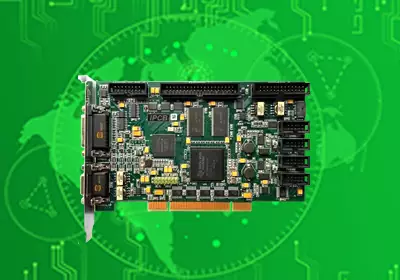

Product Name:PCB Design
Material:FR4
Thickness: 1.6mm
Copper thickness: 1/OZ
Surface technology: Enig/OSP/Hasl/Immersion gold
Solder mask: White/Black/Red/Green/Blue
Silk screen: White
Minimum line width/spacing: 3mil
Minimum through-hole: 0.3mm
Application:Printed circuit board
The pcb design is based on circuit schematics and is intended to fulfil the functional requirements of the circuit designer. The core of the design process is the layout, which requires careful consideration of the configuration of the external connections. Optimisation of the layout of the internal electronic components. Optimisation of the layout of metal connections and vias. Electromagnetic protection and heat dissipation.A good layout design can reduce production costs while ensuring excellent circuit performance and heat dissipation. Simple layout designs can be done manually,while complex layout designs can be achieved with the help of computer-aided design (CAD) tools.
PCB design should follow the rules:
1.Management of the length of the alignment: management of the length of the principle of the alignment in short, is the pursuit of short path alignment. In the PCB design process, should try to shorten the length of the alignment,in order to avoid additional interference caused by the line is too long. Especially for some critical signal lines, such as clock signal lines, it is important to place the oscillator close to the relevant device. When driving multiple devices, the topology of the network should be planned according to the specific situation.
2.Prevent the generation of self-loop alignments:In PCB design,we must be vigilant about the formation of signal lines in different layers between the self-closing loop, especially in the multilayer board wiring process, the signal line across different layers is more likely to generate self-loop, and this self-loop will cause radiation interference problems.
3.Minimise the principle of grounded loops:This principle emphasises that signal lines and the loops they form should have the smallest possible loop area. The smaller the loop area, the less energy it radiates to the outside world, and the lower the possibility of external interference. When planning the layout of the ground plane, comprehensive consideration needs to be given to the distribution of the ground plane and the location of key signal lines, so as to avoid problems brought about by factors such as the slotting of the ground plane. In the double-layer board design, while ensuring that sufficient space is allocated for the power supply, the remaining area should be filled with reference ground, and the effective connection of signals on both sides should be realised through the addition of necessary vias. For certain critical signals, especially for high-frequency designs, ground isolation measures should be prioritised. In addition, for the ground plane signal loop problem of high frequency design, it is recommended to use multi-layer board design to achieve the best results.
4.High-speed signal shielding design in the ground loop guidelines, the core purpose of the same is to minimise the signal loop area, this practice is particularly applicable to clock signals. Synchronisation signals and other important signals. In the face of extremely critical and high-frequency signals, should consider the use of copper-axis cable shielding structure layout, that is, to ensure that the signal line in the layout of the ground line is surrounded by a full range of isolation, and also need to carefully plan how to efficiently ground the shield, while maintaining isolation from the ground, and ultimately to achieve effective integration with the actual ground plane.
5.Prevent the ‘antenna effect’: In the wiring process, it is strictly prohibited one end of the overhang, the main purpose of this provision is to avoid the ‘antenna effect’, thus weakening the unnecessary interference with the radiation and reception, to prevent the unpredictable consequences that may be triggered.
6.Rounded corners design principle: In PCB design, should avoid the formation of sharp corners and right angles, because these angles may produce excess radiation, and affect the process performance. To ensure the quality of the design, the angle between all lines should be maintained at ≥135°.
7.The principle of preventing spatial overlapping of different power supply layers is mainly to reduce mutual interference between different power supplies, especially when the power supply voltage difference is significant, the problem of overlapping power supply planes must be avoided as much as possible. If it is really difficult to avoid overlapping, you can consider inserting a grounding layer between them as isolation.
8.Prevent over-hole adjacent to the SMT pads: If the over-hole is not plugged hole processing, the layout should be careful to avoid the over-hole is set too close to the SMT pads. Too close to the distance may make the solder in the SMT pad reflow through the hole penetrate to the other side of the PCB, resulting in a lack of solder, increasing the risk of false soldering and other problems. It is generally recommended to keep the distance between the edge of the vias and the SMT pads greater than 25mil, and to implement hole plugging operations for the vias.
9.Avoid the wide wire directly into the SMT pad: when the width of the wire more than the pad, usually leads to the SMT pad window area expanded beyond the size of the pad itself. This causes the exposed copper portion of the original SMT pad window to expand accordingly on the alignment, which in turn means that during reflow, if the solder paste on the pad is slightly insufficient, it may face the potential risk of false soldering. In addition, the use of larger than the pads or slightly smaller than the pads of the alignment can also be avoided during the soldering of excessive heat dissipation problems.
10.Avoid components close to the board edge layout: In the PCB assembly and soldering process, PCB boards need to be transferred between a number of process areas, such as from the solder paste coating area to the mounter, and then to the reflow soldering machine to complete the welding. Therefore, in the design of the PCB, need to ensure that at least one pair of edges on the board for the conveyor belt to reserve enough space, that is, the so-called process edge. The width of the process edge should not be less than 3mm, the length of not less than 50mm. within the scope of this process edge, components and leads must not interfere with the PCB board to avoid affecting the smooth transmission. If the layout of the PCB board can not meet this requirement, you can consider adding a separate 3mm process edge or panel to solve. (Remarks: SMT components should not be placed within 5mm from the edge of the board in order to facilitate reflow soldering operations.) Of course, this requirement can be ignored if the components on the PCB are soldered by hand and do not need to be transferred by conveyor belt.
When a collocation design is used, it should be ensured that a safe distance is maintained between the components and the edges of the V-cut lines or stamp holes. This is to prevent damage to the components during board separation or damage caused by excessive stress on the soldering discs. For PCBs that rely on machine automation for depaneling, it is required that each side of the V-CUT line (i.e., the top and bottom surfaces) retains a device prohibited area of not less than 1mm, which is to prevent damage to the device during the automated depaneling process. At the same time, it is also necessary to consider the structure of the blade of the automatic depaneling machine. Within 5mm from the boarding area of the veneer, devices with a height higher than 25mm are not allowed to be placed. When using V-CUT design, you need to consider the above two, whichever is more stringent. Ensure that the V-CUT process does not damage components and facilitates PCB separation. If the boards are connected through stamped holes, the components should be more than 100mil from the edge of the board.
11.Maintain the consistency of soldermask window size: In PCB design, package pads need to open the window on the soldermask layer, these windows to ensure that the pad area is not soldermask material (such as the commonly used green soldermask, there are also black . Red. Yellow. Blue, etc.). The main function of the soldermask is to protect the PCB circuitry from the risk of oxidation and short circuits. In order to ensure the solderability of the pads when soldering, to avoid the soldermask covered by the pads due to process errors, we usually design the soldermask openings slightly larger than the pads, generally increased by 0.1 mm (i.e., 4 mils), but you can also choose not to increase the size of the soldermask openings and the pads are consistent with the size of the factory to carry out a unified treatment. However, this requires the production of PCB packages, all the soldermask openings must be consistent in size, either exactly the same size as the pads, or uniformly larger than the pads 0.1 mm. If there are dimensional inconsistencies, such as part of the flare-out 0.05 mm, part of the flare-out 0.1 mm, will give the factory production processing to bring additional challenges.
12.Reduce EMI interference: each PCB may become a victim or source of EMI. Therefore, in the PCB layout design stage requires extra caution: increase the distance between the high-frequency alignment and low-frequency or analogue alignment to reduce mutual interference. Ensure that the return path of high-speed signals as short as possible and does not cross the split plane to reduce EMI radiation. Narrowing the current loop can effectively reduce the intensity of EMI radiation. High-speed differential signals should be wired in parallel and of equal length to avoid weakening the noise rejection capability of differential pairs. At the same time, the use of vias on high-speed alignments should be avoided as they may increase EMI emission.

Common PCB designsoftware and features
Altium Designer is a world-renowned PCB design software. Its official website describes the software as ‘Turning your ideas into reality, Altium Designer provides you with a comprehensive suite of tools designed to simplify and accelerate your design process, from schematic to PCB design and test.’ As an integrated tool suite, Altium Designer delivers a full-flow solution from conceptual ideation to manufacturing. Its powerful design utility integrates schematic design. Simulation. Schematic design. Layout. BOM management. 3D modelling and automated wiring. This full-flow solution has been labelled as an integrated design system, enabling designers to efficiently and effectively carry out the overall design.
Its advantages include:
(1) As an integrated design software, Altium Designer is fully functional, making the design process smoother.
(2) The software is compatible with more than 300 ECAD design software tools and more than 8,000 device libraries.
(3) Its 3D modelling environment is very suitable for mechanical design and other complex 3D scenarios in the design, can significantly improve the communication and collaboration between the design team efficiency.
(4) Altium Designer also has a corresponding function for embedded system design.
Cadence Allegro is a powerful commercial EDA (Electronic Design Automation) software, which, with its many advanced features, the electronic system components and PCB software for accurate control to ensure the smooth progress of the project.
Its advantages are mainly reflected in:
(1) Cadence Allegro integration of three-dimensional electronic design and simulation. PCB design and hardware description language (HDL) and a number of advanced technologies, making the workflow to a more refined control.
(2) The software is optimised for the latest DRC (Design Rule Check) requirements, which significantly improves the design efficiency.
(3) Allegro software has excellent scalability, offering a wide range of tool options in multiple versions for different types of electronic devices and applications.
However, it also has some shortcomings:
1) Higher learning costs, users need to invest some time and effort to learn, and may need technical support assistance.
2) Compared with other PCB design software, Cadence Allegro's price positioning is high.
Mentor Graphics Pads is a Mentor Graphics company by the United States to create a professional-grade PCB design software, its core concept has always been around the ‘simplify circuit board design’ as the goal.
The software has significant advantages:
(1) easy to grasp, learning difficulty is low, suitable for newcomers to get started quickly.
(2) intuitive and easy to use functional design, as a lightweight EDA tools, can effectively reduce the designer's workload.
(3) built-in a number of commonly used functions, providing users with great convenience.
(4) It supports the input and output of design files in various XCAD formats, which is suitable for diversified product application scenarios.
However, it also has some limitations:
(1) The software has relatively limited functionality and may not be able to fully meet the specific needs of complex circuit design.
(2) Components are numerous and functionally dispersed, resulting in a low level of overall integration.
KiCad: This is a free and open source design software that runs on all major operating systems. It supports the design of PCBs with up to 32 copper layers, making it ideal for building complex designs, and KiCad incorporates a comprehensive design workflow that allows users to design schematics and corresponding PCBs simultaneously, as well as independent workflows for special requirements. In addition, KiCad offers a range of useful tools, including a PCB calculator for analysing the electrical characteristics of circuit structures. Gerber Viewer for verifying manufacturing files. A 3D viewer for previewing finished PCBs and an integrated SPICE simulator for verifying circuit performance.
EAGLE:This is a beginner-oriented PCB such as design software Ger, ber known for its and simple DX easy to use F and so on. It provides prote basic us schematic: design this is a . Circuit layout design as well as automatic wiring function, while compatible with a variety of file formats, simulation software, but also has the ability to PCB design. From schematic layout . Code debugging to the co-simulation of microcontroller and peripheral circuits, Proteus is an excellent microcontroller and peripheral device simulation tools.
Product Name:PCB Design
Material:FR4
Thickness: 1.6mm
Copper thickness: 1/OZ
Surface technology: Enig/OSP/Hasl/Immersion gold
Solder mask: White/Black/Red/Green/Blue
Silk screen: White
Minimum line width/spacing: 3mil
Minimum through-hole: 0.3mm
Application:Printed circuit board
iPCB Corporation provides support for PCB Prototype and Electronic Manufacturing. You can request consultation or quotation for PCB, PCBA and ODM here, please contact email: sales@ipcb.com
We will respond very quickly.